Unlock instant, AI-driven research and patent intelligence for your innovation.

Manufacturing method of dynamic random access memory

A technology of dynamic random access and manufacturing methods, which is applied in the field of memory, can solve problems such as the complexity of the manufacturing method of dynamic random access memory, and achieve the effects of reducing process complexity, improving storage capacity, and improving stability

Inactive Publication Date: 2018-08-21
CHANGXIN MEMORY TECH INC
View PDF7 Cites 0 Cited by
  • Summary
  • Abstract
  • Description
  • Claims
  • Application Information

AI Technical Summary

Problems solved by technology

[0007] In view of the above-mentioned shortcomings of the prior art, the object of the present invention is to provide a method for manufacturing a DRAM, which is used to solve the problem that the manufacturing method of the DRAM is complicated in the prior art

Method used


Image

  • Manufacturing method of dynamic random access memory
  • Manufacturing method of dynamic random access memory
  • Manufacturing method of dynamic random access memory

Examples


Embodiment 1

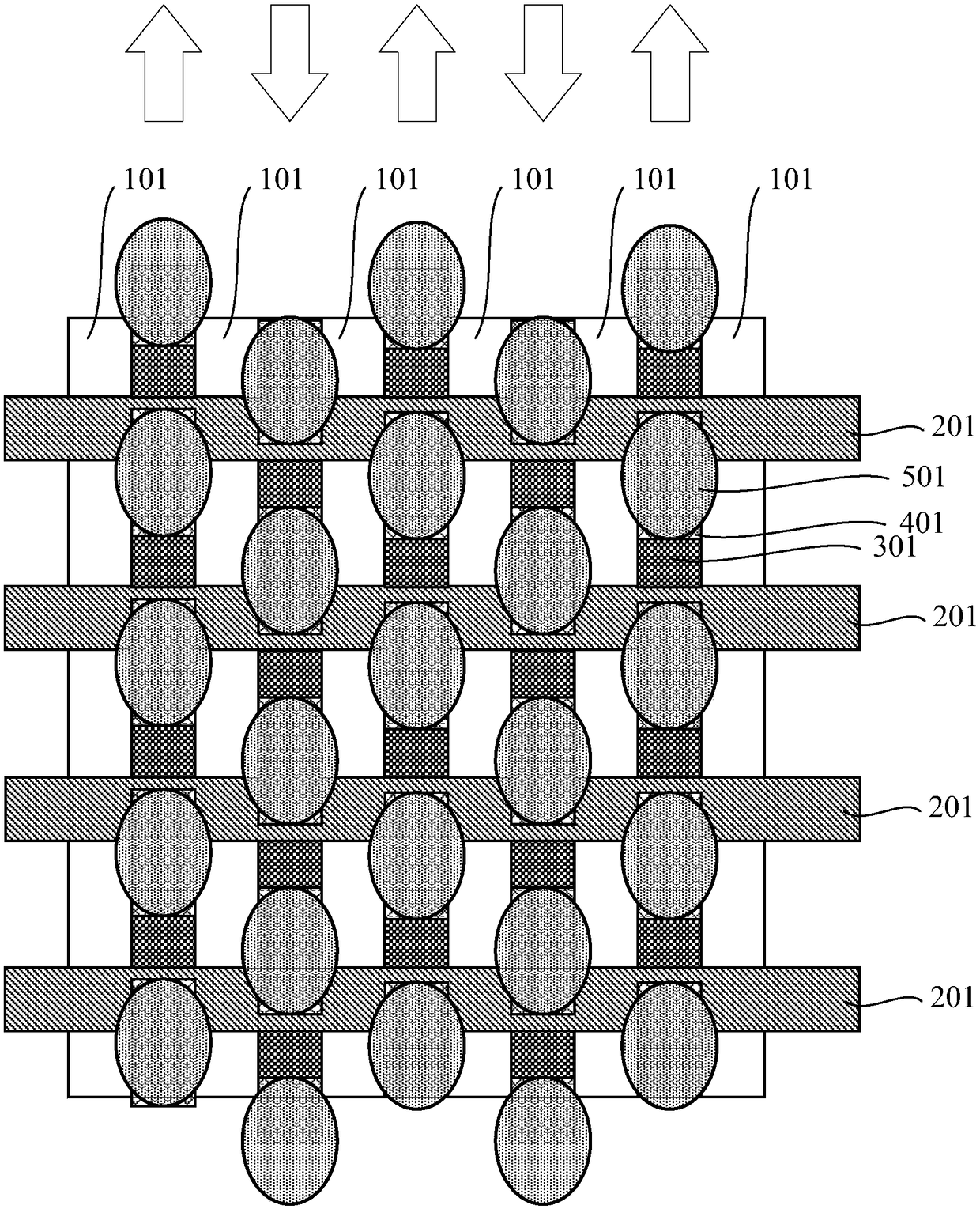
[0105] The present invention prepares a dynamic random access memory. The dynamic random access memory includes a word line array, a bit line array, a contact plug array, a contact pad array and a capacitor array. among them, figure 1 Shown as a plane layout diagram of the dynamic random access memory. In order to clearly show the arrangement of each array and the relative position relationship between different arrays, figure 2 , image 3 , Figure 7 , Picture 8 , Picture 9 Shown as the respective planar layout diagrams of the word line array 1, the bit line array 2, the contact plug array 3, the contact pad array 4, and the capacitor array 5. Figure 4 Shown as a common plan layout of the word line array 1 and the bit line array 2, Figure 5 Shown as a common plan layout of the word line array 1, bit line array 2 and contact plug array 3, Image 6 Shown as a plane layout diagram of the word line array 1, the bit line array 2, the contact plug array 3, and the contact pad arr...

Embodiment 2

[0126] The present invention also provides a method for manufacturing a dynamic random access memory, which includes the following steps: first please refer to Figure 16 , Perform steps S1 and S2: provide a semiconductor structure 100 that includes a substrate 8, a multilayer film structure 9 on the upper surface of the substrate 8, and a contact on the upper surface of the multilayer film structure 9 Land 401. A passivation layer 10 covering the contact pad is formed on the upper surface of the semiconductor structure 100. As an example, the material of the passivation layer 10 includes any one or a combination of any two or more of silicon nitride, silicon oxynitride, and aluminum oxide.

[0127] Then see Figure 17 , Step S3 is performed: a first sacrificial layer 11, a first supporting layer 12, a second sacrificial layer 13, and a second supporting layer 14 are sequentially formed on the passivation layer 10.

[0128] Specifically, the first sacrificial layer 11 and the seco...


PUM


Abstract

The invention provides a manufacturing method of a dynamic random access memory, which comprises the following steps of: preparing a word line array, a bit line array, a contact plug array, a contactpad array and a capacitor array of a dynamic random access memory; each contact pad is connected with the upper part of the contact plug. The offset directions of the adjacent two rows of contact padsare opposite, so that the array of the contact pads is hexagonal; each capacitor is connected with the upper part of the contact pad. According to the dynamic random access memory, the planar layoutstructure is transformed into the hexagonal arrangement of the capacitors from the tetragonal arrangement of the contact plugs, so that the area of the capacitor in the storage unit can be improved and a larger capacitance value can be obtained. According to the invention, while the hexagonal layout of the capacitor and the area of the memory unit of 6F2 are realized, the active area, the word line and the bit line are all linear. The layout is simpler, the process complexity is reduced, and the stability of the memory is improved.

Description

Technical field [0001] The invention belongs to the memory field and relates to a manufacturing method of a dynamic random access memory. Background technique [0002] A capacitor is a passive electronic component that stores energy in the form of an electrostatic field. In the simplest form, a capacitor includes two conductive plates, and the two conductive plates are separated by an insulating material called a dielectric. The capacitance of a capacitor is directly proportional to the surface area of ​​the plates and inversely proportional to the distance between the plates. The capacitance of a capacitor also depends on the dielectric constant of the material separating the plates. [0003] The standard unit of capacitance is farad (abbreviated as F), which is a large unit, and the more common units are microfarad (abbreviated as μF) and picofarac (abbreviated as PF), among which 1 μF = 10 -6 F, 1pF=10 -12 F. [0004] Capacitors can be manufactured on integrated circuit (IC) ch...

Claims


Application Information

Patent Timeline
Patent Type & Authority Applications(China)
IPC IPC(8): H01L27/11568H10B12/00H10B43/30
CPCH10B12/30H10B12/03H10B43/30
Inventor 不公告发明人
Owner CHANGXIN MEMORY TECH INC
Features
  • R&D
  • Intellectual Property
  • Life Sciences
  • Materials
  • Tech Scout
  • Unparalleled Data Quality
  • Higher Quality Content
  • 60% Fewer Hallucinations
Learn More