A circuit fixing device for potential-induced degradation circuit layout in a photovoltaic module

A fixed device, potential-induced technology, applied in photovoltaic modules, photovoltaic power generation, electrical components, etc., can solve the problems of blurred deterioration results, inability to subdivide the types of deterioration clearly, and mechanism attenuation, etc., to achieve the effect of convenient placement.

Active Publication Date: 2019-07-16
中达安股份有限公司
View PDF6 Cites 0 Cited by
  • Summary
  • Abstract
  • Description
  • Claims
  • Application Information

AI Technical Summary

Problems solved by technology

[0004] The purpose of the present invention is to provide a circuit fixing device for potential-induced degradation circuit layout in photovoltaic modules, so as to solve the problem of the existing photovoltaic module potential-induced degradation arrangement proposed in the background technology, the circuit is usually fixed by integrated sealing way, this fixing method increases the steps and time required for the entire layout, so that the layout takes too long, and the degradation effect cannot be realized faster, and the placement of the entire fixing device is not adjusted according to the specific degradation effect induced by the module, so that Crystalline silicon photovoltaic modules cannot better perform selective heating and corrosion degradation, resulting in the attenuation of the mechanism, so that the types of degradation cannot be subdivided clearly, which affects the experimental classification of degradation results and makes the degradation results blurred

Method used


Image

  • A circuit fixing device for potential-induced degradation circuit layout in a photovoltaic module
  • A circuit fixing device for potential-induced degradation circuit layout in a photovoltaic module
  • A circuit fixing device for potential-induced degradation circuit layout in a photovoltaic module

Examples


Embodiment Construction

[0021] The following will clearly and completely describe the technical solutions in the embodiments of the present invention with reference to the accompanying drawings in the embodiments of the present invention. Obviously, the described embodiments are only some, not all, embodiments of the present invention. Based on the embodiments of the present invention, all other embodiments obtained by persons of ordinary skill in the art without making creative efforts belong to the protection scope of the present invention.

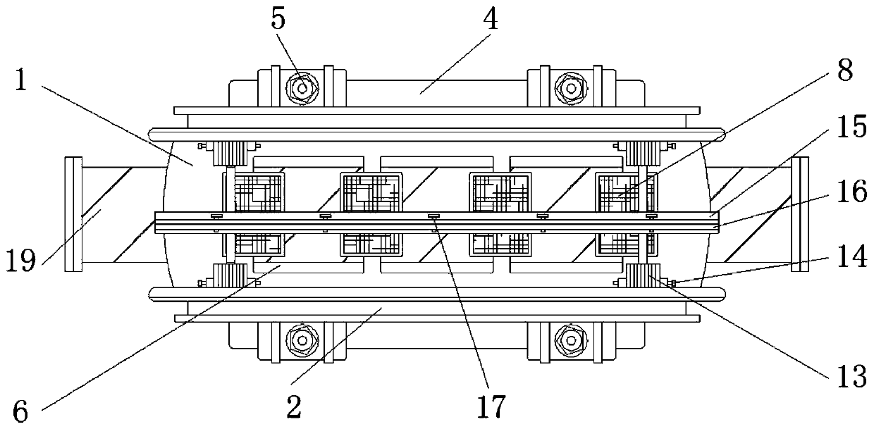
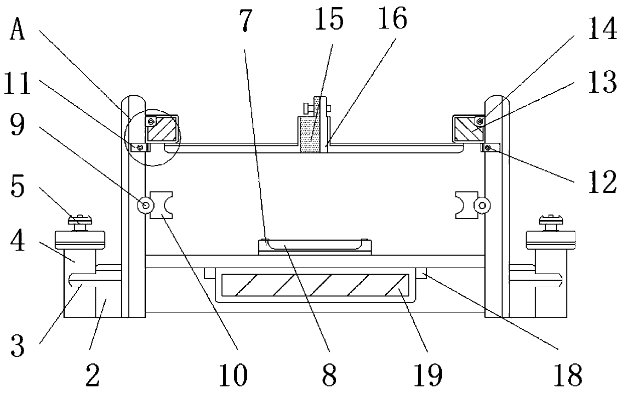
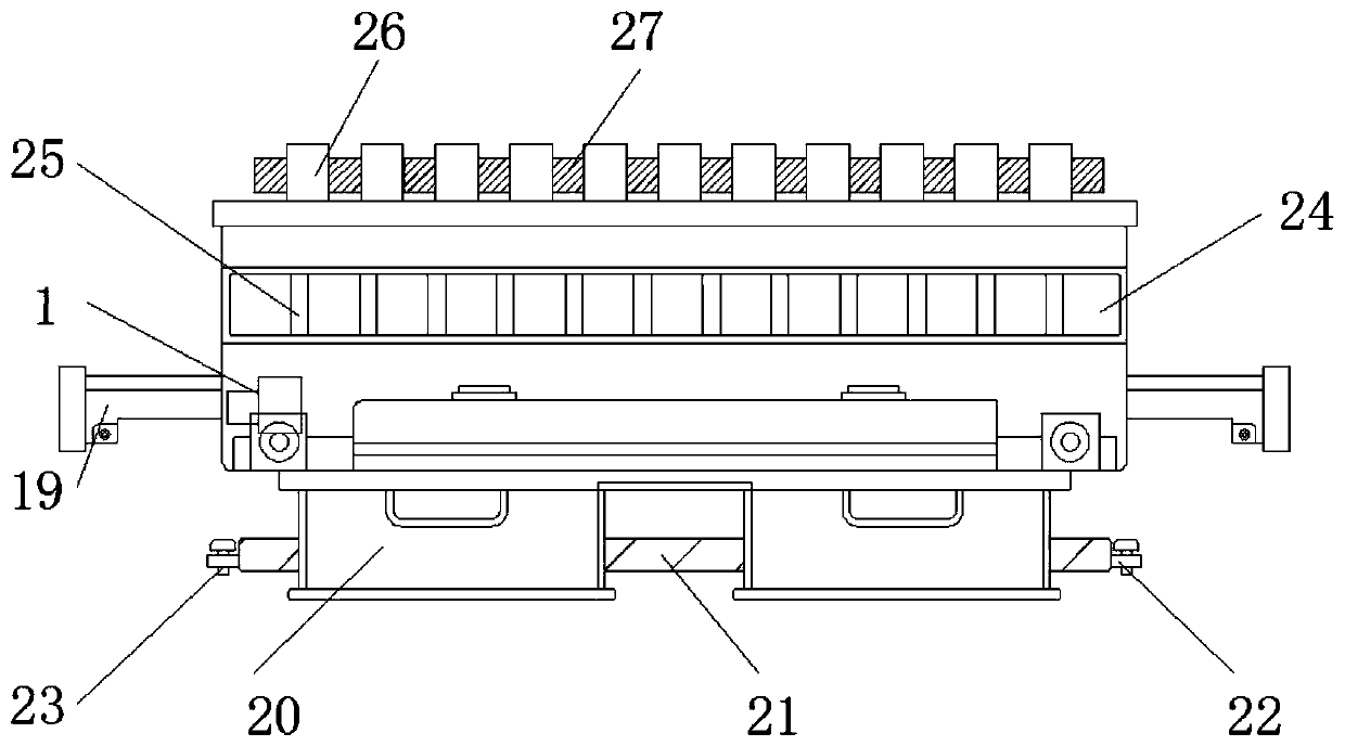
[0022] see Figure 1-5, the present invention provides a technical solution: a circuit fixing device for potential-induced degradation circuit layout in a photovoltaic module, including a fixing device body 1, a fixing platform 2, a fixing bar 3, a connecting platform 4, connecting bolts 5, and cooling holes 6 , connecting groove block 7, ground metal block 8, rotating shaft 9, slot block 10, fixing gasket 11, fixing bolt 12, crystal assembly 13, through bolt ...


PUM


Abstract

The invention relates to a line fixing device for potential-induced deterioration circuit arrangement in a photovoltaic module, which comprises a fixing device body, a rotation shaft and a fixing groove, wherein the front end and the rear end of the fixing device body are fixed with fixing tables; the outer side of each fixing table is connected with a fixing bar; the outer side of the fixing baris provided with a connection table; a connection bolt passes through the upper end of the connection table; the bottom part of the fixing device body is fixed with cooling holes; and the upper end inside the fixing device body is connected with a connection groove block. According to the line fixing device for potential-induced deterioration circuit arrangement in the photovoltaic module, the connection table enables the placement width of the fixing device body to be increased, and thus, the device can be better adapted to arrangement sites with different realization effects; the connectiongroove block and a grounding metal block form a mobile structure, and according to current potential high-voltage deterioration reaction result demands under experimental detection, the connection groove block and the grounding metal block can be fixedly connected, and due to an insulation cover, a circuit mechanism response can not leak out.

Description

technical field [0001] The invention relates to the technical field of photovoltaic module potential induction, in particular to a circuit fixing device for potential-induced degradation circuit layout in photovoltaic modules. Background technique [0002] Photovoltaic is the abbreviation of solar photovoltaic power generation system. It is a new type of power generation system that uses the photovoltaic effect of solar cell semiconductor materials to directly convert solar radiation energy into electrical energy. There are two modes of independent operation and grid-connected operation. In photovoltaic The high voltage between the circuit in the crystalline silicon photovoltaic module and its grounded metal frame in the module will cause the continuous attenuation of the photovoltaic performance of the module. This phenomenon is the degradation phenomenon. [0003] In the existing photovoltaic module potential-induced degradation arrangement, the circuit is mostly fixed by ...

Claims


Application Information

Patent Timeline
Patent Type & Authority Patents(China)
IPC IPC(8): H02S40/30
CPCH02S40/30Y02E10/50
Inventor 罗均陈长青林家威
Owner 中达安股份有限公司
Why Eureka
Try Eureka