Transistor and preparation method thereof

A transistor and modulation technology, which is applied in the field of transistors and their preparation, can solve problems such as poor reliability and characteristic degradation, and achieve the effects of reducing electric field strength, improving device reliability, and avoiding device characteristic degradation

Inactive Publication Date: 2018-08-24
INNOSCIENCE (ZHUHAI) TECH CO LTD
View PDF5 Cites 4 Cited by
  • Summary
  • Abstract
  • Description
  • Claims
  • Application Information

AI Technical Summary

Problems solved by technology

[0005] The present invention at least partly solves the problems of characteristic degradation and poor reliability of existing transistors provided with a P-type cap layer as they are used, and provides a transistor that can avoid characteristic degradation and has good reliability

Method used


Image

  • Transistor and preparation method thereof
  • Transistor and preparation method thereof
  • Transistor and preparation method thereof

Examples


Embodiment 1

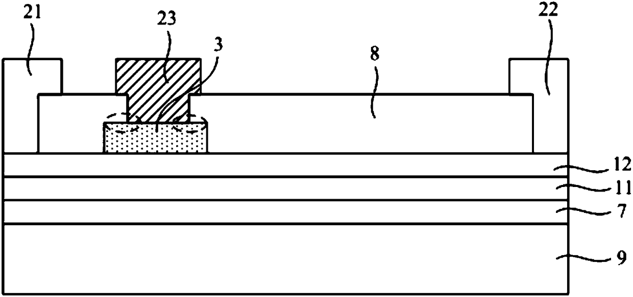
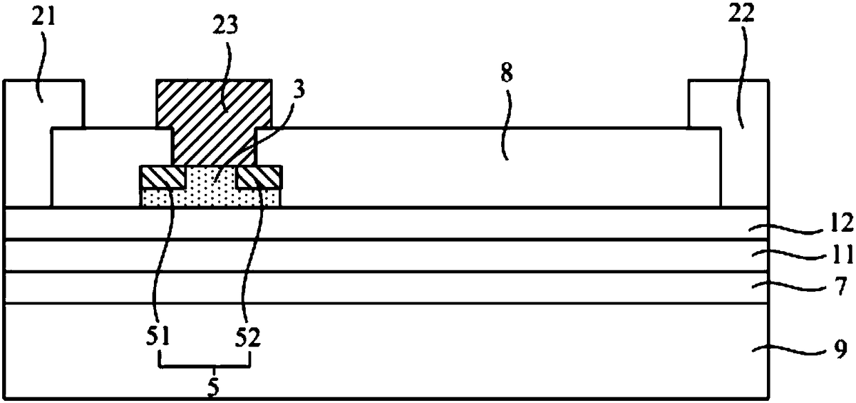
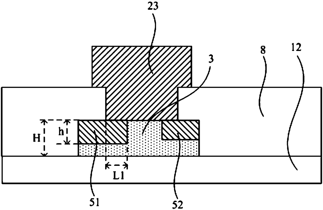
[0039] Such as Figure 2 to Figure 7 As shown, this embodiment provides a transistor, which includes:

[0040] stacked channel layer 11 and barrier layer 12;

[0041] The source 21, the drain 22, and the gate 23 are arranged at intervals on the side of the barrier layer 12 away from the channel layer 11; wherein, the gate 23 is located between the source 21 and the drain 22, and is provided between the barrier layer 12 There is a P-type cap layer 3, and a Schottky contact is formed between the P-type cap layer 3 and the gate 23;

[0042] Such as figure 2 As shown, the transistor of this embodiment includes a stacked channel layer 11 and a barrier layer 12, a heterojunction is formed between the channel layer 11 and the barrier layer 12, and the barrier layer 12 has a larger forbidden band width , so that a two-dimensional electron gas (2DEG) can be formed on the side of the heterojunction interface close to the channel layer 11 . On the side of the barrier layer 12 away f...


PUM


Abstract

The invention provides a transistor and a preparation method thereof, belongs to the technical field of transistors (especially gallium nitride transistors) and is capable of at least partially solving the problems of characteristic degradation and poor reliability of an existing transistor provided with a P-type cap layer along with use. The transistor provided by the invention comprises superimposed channel layer and barrier layer, a source, a drain and a gate, wherein the source, the drain and the gate are arranged at one side, far away from the channel layer, of the barrier layer at intervals; the gate is located between the source and the drain; the P-type cap layer is arranged between the gate and the barrier layer; schottky contact is formed between the P-type cap layer and the gate; two side edge areas, close to the source and the drain, of the P-type cap layer are two interspaced electric field modulation areas; and the electric field modulation areas can induce positive charges under positive gate-source voltage.

Description

technical field [0001] The invention belongs to the technical field of transistors (especially gallium nitride transistors), and in particular relates to a transistor and a preparation method thereof. Background technique [0002] Gallium nitride (GaN) semiconductor has the characteristics of large band gap, high breakdown voltage, high electron saturation and high drift speed, so GaN transistors prepared with it have high breakdown voltage, low on-resistance, and fast response speed. And other advantages, especially suitable as a switching device. [0003] Such as figure 1 As shown, in order to improve the performance of the gallium nitride transistor to form an enhanced gallium nitride high electron mobility transistor (GaN HEMT, E-mode GaN High Electron Mobility Transistor), the gate 23 and the barrier layer 12 can be A P-type cap layer 3 (P-Cap) is inserted between them. But for such gallium nitride transistors, when the positive gate-source voltage reaches a certain ...

Claims


Application Information

Patent Timeline
Patent Type & Authority Applications(China)
IPC IPC(8): H01L29/778H01L21/335
CPCH01L29/66462H01L29/7786H01L29/2003H01L29/1066H01L29/207H01L29/0607H01L21/2654H01L29/205
Inventor 魏进金峻渊
Owner INNOSCIENCE (ZHUHAI) TECH CO LTD
Why Eureka
Try Eureka