Grating LED (light-emitting diode) chip and preparation method

A technology of LED chip and manufacturing method, which is applied in the direction of electrical components, circuits, semiconductor devices, etc., and can solve the problems of low brightness of the chip, too large difference in refractive index, and inability to emit light from the chip.

Inactive Publication Date: 2018-08-24
YANGZHOU CHANGELIGHT
View PDF1 Cites 2 Cited by
  • Summary
  • Abstract
  • Description
  • Claims
  • Application Information

AI Technical Summary

Problems solved by technology

[0004] However, at present, the surface of the epitaxial layer structure of the chip in contact with the air has a problem that the refractive index difference is too large, causing most of the light from the chip to be unable to emit, so that the brightness of the chip is low

Method used


Image

  • Grating LED (light-emitting diode) chip and preparation method
  • Grating LED (light-emitting diode) chip and preparation method
  • Grating LED (light-emitting diode) chip and preparation method

Examples


Embodiment Construction

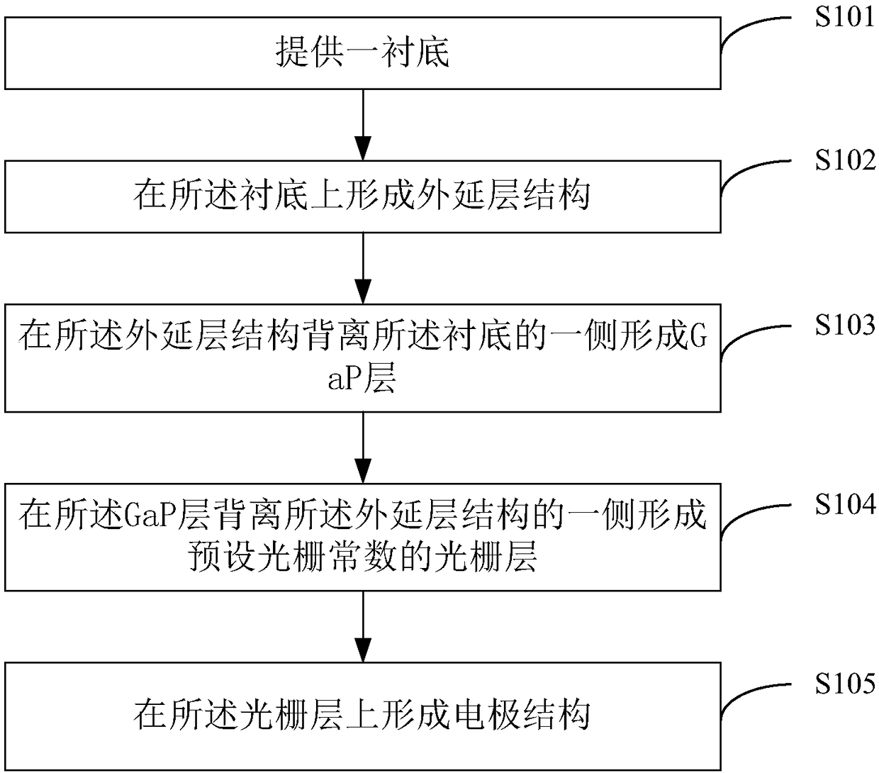
[0046] The following will clearly and completely describe the technical solutions in the embodiments of the present invention with reference to the accompanying drawings in the embodiments of the present invention. Obviously, the described embodiments are only some, not all, embodiments of the present invention. Based on the embodiments of the present invention, all other embodiments obtained by persons of ordinary skill in the art without making creative efforts belong to the protection scope of the present invention.

[0047] In order to make the above objects, features and advantages of the present invention more comprehensible, the present invention will be further described in detail below in conjunction with the accompanying drawings and specific embodiments.

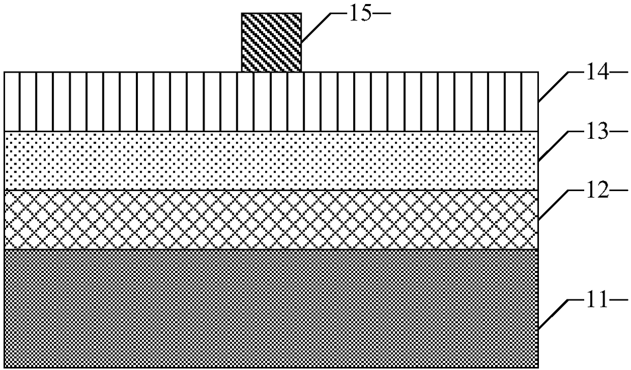
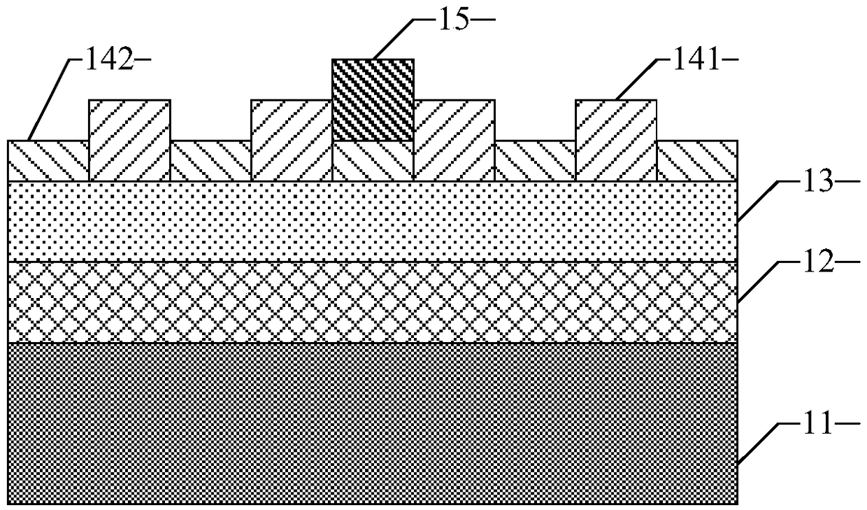
[0048] refer to figure 1 , figure 1 It is a schematic structural diagram of a grating LED chip provided by an embodiment of the present invention.

[0049] The grating LED chip includes: a substrate 11; an epita...


PUM


Abstract

The invention discloses a grating LED (light-emitting diode) chip and a preparation method. The grating LED chip comprises a substrate; an epitaxial layer structure arranged on the substrate; a GaP layer arranged at one side, departing from the substrate, of the epitaxial layer structure; a grating layer with preset grating constant arranged at one side, departing from the epitaxial layer structure, of the GaP layer; and an electrode structure arranged on the grating layer. The grating LED chip is high in luminous efficiency, large in luminous area, and high in brightness.

Description

technical field [0001] The invention relates to the technical field of LED chip manufacturing, and more specifically, to a grating LED chip and a manufacturing method. Background technique [0002] With the continuous development of science and technology, various LED chips have been widely used in people's daily life, work and industry, bringing great convenience to people's life. [0003] Light Emitting Diode (LED) has many advantages such as high efficiency, low energy consumption, long life, no pollution, small size, rich colors, etc., and is widely used in lighting, display, backlight and other fields. [0004] However, at present, the surface of the epitaxial layer structure of the chip in contact with the air has a problem that the refractive index difference is too large, which prevents most of the light from the chip from being emitted, so that the brightness of the chip is low. [0005] Then, how to provide a chip with high light extraction efficiency, large light...

Claims


Application Information

Patent Timeline
Patent Type & Authority Applications(China)
IPC IPC(8): H01L33/44H01L33/30H01L33/00
CPCH01L33/44H01L33/005H01L33/30
Inventor 赵炆兼贾钊曹广亮郭冠军王宇
Owner YANGZHOU CHANGELIGHT
Why Eureka
Try Eureka