Eureka AIR delivers breakthrough ideas for toughest innovation challenges, trusted by R&D personnel around the world.

Neuro-inspired all-optical memory device based on ge2sb2te5

A memory and device technology, applied in the field of picosecond laser applications, can solve problems such as energy waste, obvious current heating effect, and increasing CPU processor density.

Active Publication Date: 2020-07-03
BEIJING UNIV OF TECH
View PDF4 Cites 0 Cited by
  • Summary
  • Abstract
  • Description
  • Claims
  • Application Information

AI Technical Summary

Problems solved by technology

[0006] Today's computers mainly use electrical signals, but as the width of the wires decreases, the heating effect of the current becomes more and more obvious, resulting in serious energy waste
And as the line width decreases, the electron tunneling effect leads to a serious obstacle to further increase the CPU processor density.

Method used


Image

  • Neuro-inspired all-optical memory device based on ge2sb2te5
  • Neuro-inspired all-optical memory device based on ge2sb2te5
  • Neuro-inspired all-optical memory device based on ge2sb2te5

Examples


Embodiment Construction

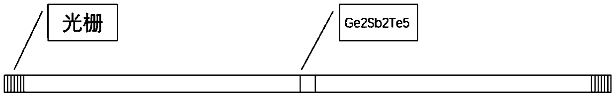
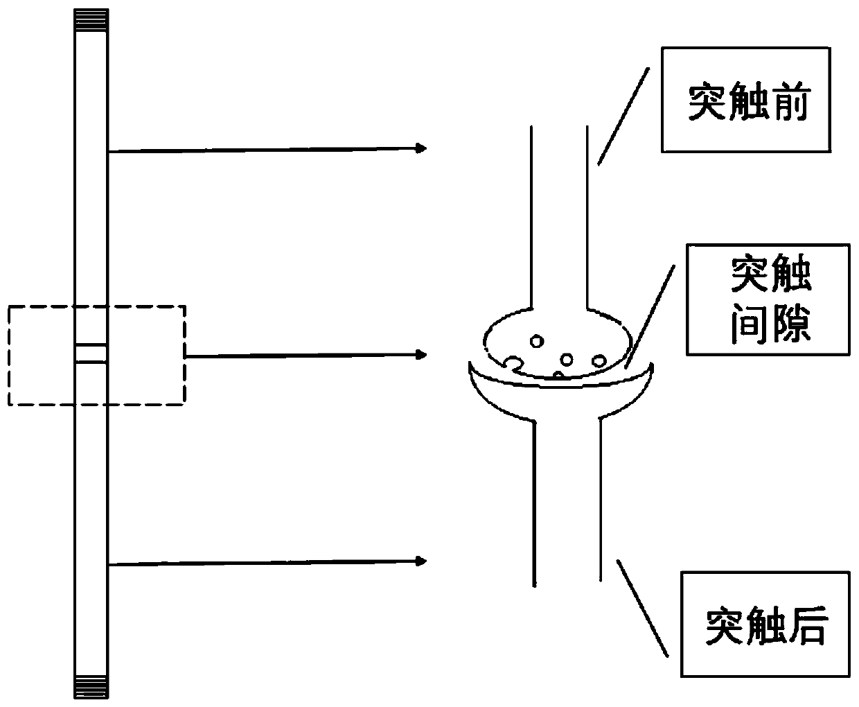
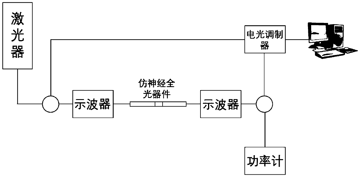
[0027] The present invention will be further described below in conjunction with the examples, but the present invention is not limited to the following examples. Such as image 3 , as shown in the schematic diagram of the work of the neuromimetic all-photonic memory device, the device is composed of the following parts: 1. Picosecond laser, this experiment uses the picosecond laser produced by EKSPLA company, the central wavelength is 1064nm, and the light intensity distribution is Gaussian type, linearly polarized. 2. The photoelectric modulator, which adjusts the light pulse input from the right end of the optical waveguide through the photoelectric modulator, and adjusts the time difference between the two beams of light pulses in the coupling area. 3. Power meter, which detects the change of light energy passing through the optical waveguide through the power meter, so as to reflect the change of transmittance caused by the coupling between Ge2Sb2Te5 and the optical wave...


PUM

PropertyMeasurementUnit
refractive indexaaaaaaaaaa

Abstract

The invention discloses a neuron-like all-optical memory device based on Ge2Sb2Te5, and belongs to the technical field of picosecond laser application. The neuron-like all-optical memory device is based on a multi-pulse action and an STDP neural memory theory. The amorphous Ge2Sb2Te5 is coupled with optical waveguide. Ge2Sb2Te5 is attached to the optical waveguide by a way of magnetron sputtering,and a coupling region is a bionic neural synaptic cleft. The device can realize the reading, memory and erasing processes of the device through all-optical signals. Moreover, the refractive index ofcrystalline Ge2Sb2Te5 is higher than that of amorphous Ge2Sb2Te5, so the material after crystallization is easier to deflect to the direction of Ge2Sb2Te5 than that of amorphous light, the informationretention in the memory region is facilitated, and the device continuously strengthens recording in use.

Description

technical field [0001] The invention relates to a bionic memory device based on a phase-change material Ge2Sb2Te5, which uses a picosecond laser as an energy and signal generation source, and belongs to the technical field of picosecond laser applications. Background technique [0002] In computer science, computers make extensive use of Neumann structures. That is, the input information is coded by the CPU, stored in a certain location of the memory, and the information is extracted from the memory when the data is used, which causes information to frequently go back and forth between the CPU and the memory. Due to the limitation of the bandwidth between the memory and the CPU, the computing speed of the CPU is much faster than the speed of information going back and forth between the memory and the CPU, resulting in a decrease in the actual computing speed and an increase in power consumption. This is called the Neumann bottleneck. When performing simple calculations that...

Claims


Application Information

Patent Timeline
Patent Type & Authority Patents(China)
IPC IPC(8): G11C13/04
CPCG11C13/047
Inventor 刘富荣韩子豪樊婷韩钊黄引张永志
Owner BEIJING UNIV OF TECH
Why Eureka
Eureka Blog
Learn More