Method and apparatus for improved singulation of light emitting devices

a technology of light emitting devices and singulation methods, applied in laser beam welding apparatus, manufacturing tools, welding/soldering/cutting articles, etc., can solve the problems of reducing light output, reducing light output, and diminishing light output, so as to reduce the amount of thermal debris, improve light output, and control the effect of heat damage to the substra

Inactive Publication Date: 2012-07-12
ELECTRO SCI IND INC
View PDF1 Cites 25 Cited by
  • Summary
  • Abstract
  • Description
  • Claims
  • Application Information

AI Technical Summary

Benefits of technology

[0009]Aspects of this invention improve light output from singulated light emitting devices by using laser pulse parameters that reduce the amount of thermal debris and control the heat damage to the substrate. Laser pulses with 532 nm wavelength, or shorter, with pulse widths of less than about 10 ps emitted at a pulse repetition in the 75 kHz to 800 kHz range are advantageously used to scribe sapphire substrates. The laser pulses are delivered to the substrate using an adapted laser scribing system. These pulses are focused to a less than about 1 micron to about 5 micron focal spot which is positioned with respect to the substrate by cooperation between the adapted laser scribing system's beam positioning optics and the motion control stages. The laser parameters are adjusted so that desirable changes in substrate materials occur in and adjacent to the focal spot and minimum undesirable changes occur in the material around the focal spot. Desirable effects of the laser pulses include altering the molecular or crystalline structure of the material to enhance crack initiation or propagation and providing a predetermined amount of texture to the irradiated edge following cleaving. By properly selecting laser pulse parameters, the modifications made to the substrate materials can enhance crack initiation and propagation so that reduced mechanical force is required to cleave the material following laser scribing, thereby reducing the chances of chipping and other undesirable effects of cleaving. Further undesirable effects include damage caused by a heat affected zone (HAZ) near the irradiated location and thermal debris. HAZ damage includes creation of microcracks which reduce die break strength and creation of edge regions which absorb and reflect light back into the device, thereby reducing light output. Thermal debris also absorbs and reflects light back into the device, also reducing light output. Aspects of this invention employ laser parameters which promote the formation of modified regions in the substrate with just enough deteriorated or modified materials to form a textured surface which promotes light transmission through the sidewalls but does not extend far enough laterally to inhibit light transmission.

Problems solved by technology

Further undesirable effects include damage caused by a heat affected zone (HAZ) near the irradiated location and thermal debris.
HAZ damage includes creation of microcracks which reduce die break strength and creation of edge regions which absorb and reflect light back into the device, thereby reducing light output.
Thermal debris also absorbs and reflects light back into the device, also reducing light output.
Cleaving performed on substrates with interior scribes without surface scribes tend to propagate cracks in random directions towards the surface, causing multiple facets which are defined as small regions of the edge with a common surface orientation.
These multiple random facets tend to reflect more light back into the singulated device thereby diminishing light output.

Method used


Image

  • Method and apparatus for improved singulation of light emitting devices
  • Method and apparatus for improved singulation of light emitting devices
  • Method and apparatus for improved singulation of light emitting devices

Examples


Embodiment Construction

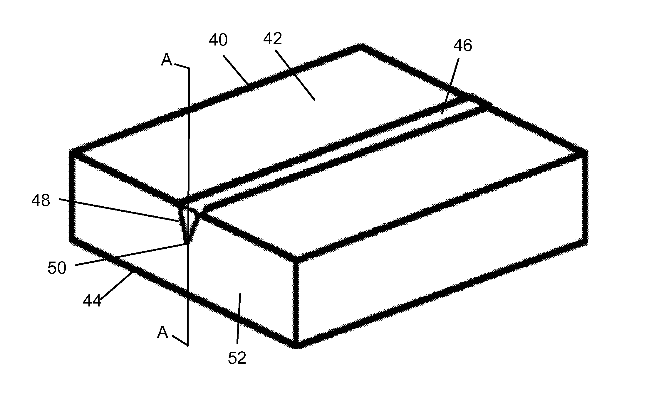
[0017]Aspects of this invention perform laser assisted singulation of light emitting electronic devices manufactured on a substrate with a laser processing system. The laser processing system uses a pulsed picosecond laser having controllable laser parameters to form a modified region on the surface of the substrate which extends into the interior of the substrate, the laser parameters being controlled to limit the extent of the modified region laterally. The substrate is then singulated by applying mechanical stress to the substrate proximate to the modified region thereby cleaving the substrate along facets which include the modified regions. These facets which include modified materials improve the light output from the light emitting device by providing a highly transmissive, diffuse, non-specular sidewall surface which improves the transmission of light from the interior of the device to the outside. Light which is reflected back into the device is undesirable first because it ...


PUM

PropertyMeasurementUnit
wavelengthaaaaaaaaaa
focal spot sizeaaaaaaaaaa
focal spot speedaaaaaaaaaa

Abstract

The present invention is a system and method for laser-assisted singulation of light emitting electronic devices manufactured on a substrate, having a processing surface and a depth extending from the processing surface. It includes providing a laser processing system having a picosecond laser having controllable parameters; controlling the laser parameters to form light pulses from the picosecond laser, to form a modified region having a depth which spans about 50% of the depth and substantially including the processing surface of the substrate and having a width less than about 5% of the region depth; and, singulating the substrate by applying mechanical stress to the substrate thereby cleaving the substrate into said light emitting electronic devices having sidewalls formed at least partially in cooperation with the linear modified regions.

Description

TECHNICAL FIELD[0001]The present invention relates to laser-assisted singulation of light emitting devices manufactured on a common substrate. Particularly, this invention relates to singulation of light emitting devices using a picosecond laser directed to create modified regions which begin on the surface of the substrate in alignment with the modified regions and extend into the interior. More particularly, this invention relates to singulation of light emitting devices having textured surfaces to enhance the light emitting properties of the devices.BACKGROUND OF THE INVENTION[0002]Electronic devices are typically manufactured by building multiple copies of the device in parallel on a common substrate and then separating or singulating the devices into separate units. The substrates include wafers of silicon or sapphire combined with layers of metallic (conducting), dielectric (insulating), or semi-conducting materials to form electronic devices. FIG. 1 shows a typical wafer 10 s...

Claims


Application Information

Patent Timeline
Patent Type & Authority Applications(United States)
IPC IPC(8): H01L33/22B23K26/00H01L21/268
CPCB23K26/0084B23K26/0087B23K26/041H01L33/0095B23K26/083B23K26/1405B23K26/4075B23K26/0635B23K26/042B23K26/0624B23K26/142B23K26/40B23K26/359B23K26/355B23K2103/50
Inventor CHYR, IRVINGHALDERMAN, JONATHANCHACIN, JUAN
Owner ELECTRO SCI IND INC
Why Eureka
Try Eureka