SMT patching process

A process and patch technology, applied in metallurgical bonding, electrical components, printed circuit manufacturing, etc., can solve the problems of heat resistance and different cooling speeds, affecting the welding quality of circuit boards, etc., to overcome slow cooling speed and ensure production quality , the effect of improving quality

Inactive Publication Date: 2018-09-11
贵州贵安新区众鑫捷创科技有限公司
View PDF3 Cites 21 Cited by
  • Summary
  • Abstract
  • Description
  • Claims
  • Application Information

AI Technical Summary

Problems solved by technology

[0002] Since entering the 21st century, China's electronic information product manufacturing industry has accelerated its pace of development and has become a pillar industry of the national economy. With the rapid development of the electronic manufacturing industry, China's surface mount technology and industry have also developed rapidly, and the overall scale is also the largest. The forefront of the world, the pursuit of miniaturization of electronic products, the perforated components used in the past can no longer be reduced, resulting in more and more stringent technical requirements for soldering, the quality of solder paste in the process of silk screen printing, placement and reflow soldering det...

Method used


Image

  • SMT patching process
  • SMT patching process
  • SMT patching process

Examples


Embodiment 1

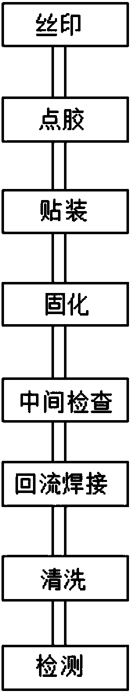
[0028] Such as Figure 1-3 As shown, a SMT patching process includes the following steps: S1, silk screen, after the circuit board is detected correctly by an optical camera, the circuit board is pasted under the stencil, and then the screen printing machine applies the solder paste or patch glue Missing printing on the pad of PCB to prepare for the soldering of components;

[0029] S2, glue dispensing, the circuit board after the screen printing step is completed, the glue is dripped onto the fixed position on the circuit board through the action of the glue dispenser, so that the electrical components are fixed on the circuit board;

[0030] S3, Mounting, sending the circuit board after the dispensing step into the placement machine, and the placement machine accurately installs the assembled components on the circuit board to a fixed position on the circuit board;

[0031] S4, curing, sending the mounted circuit board into the curing furnace, the curing furnace melts the p...

Embodiment 2

[0038] A kind of SMT placement process, comprising the following steps: S1, silk screen, after the circuit board is detected by an optical camera, the circuit board is pasted under the stencil, and then the silk screen printing machine leaks the solder paste or patch glue onto the On the pad of PCB, prepare for the soldering of components;

[0039] S2, glue dispensing, the circuit board after the screen printing step is completed, the glue is dripped onto the fixed position on the circuit board through the action of the glue dispenser, so that the electrical components are fixed on the circuit board;

[0040] S3, Mounting, sending the circuit board after the dispensing step into the placement machine, and the placement machine accurately installs the assembled components on the circuit board to a fixed position on the circuit board;

[0041] S4, curing, sending the mounted circuit board into the curing furnace, the curing furnace melts the patch adhesive, and bonds the assembl...

Embodiment 3

[0048] A kind of SMT placement process, comprising the following steps: S1, silk screen, after the circuit board is detected by an optical camera, the circuit board is pasted under the stencil, and then the silk screen printing machine leaks the solder paste or patch glue onto the On the pad of PCB, prepare for the soldering of components;

[0049] S2, glue dispensing, the circuit board after the screen printing step is completed, the glue is dripped onto the fixed position on the circuit board through the action of the glue dispenser, so that the electrical components are fixed on the circuit board;

[0050] S3, Mounting, sending the circuit board after the dispensing step into the placement machine, and the placement machine accurately installs the assembled components on the circuit board to a fixed position on the circuit board;

[0051]S4, curing, sending the mounted circuit board into the curing furnace, the curing furnace melts the patch adhesive, and bonds the assembly...


PUM


Abstract

The invention discloses an SMT patching process which comprises the following steps: S1, silk screening: patching a circuit board to the lower surface of a steel screen after an optical camera detectsthat the circuit board is free of errors, then printing soldering paste or patch leaked glue to a welding plate of a PCB through a screening printer to be prepared for welding of components; S2, gluedispensing: dropping glue to a fixed position of the circuit board after the step of silk screening by means of action of a glue dispenser, wherein the electric components are fixed to the circuit board; and S3, pasting: feeding the circuit board after the step of glue dispensing to a chip mounter. The SMT patching process has the beneficial effects that influence of environmental factors is avoided by controlling the environmental factors in the whole process technology well, so that the viscosity of solder paste can be improved; meanwhile, metal powder in the solder paste is changed to overcome the condition that original cooling speed is small and the surface of the solder paste is not steady; and furthermore, the quality of the circuit board is enhanced.

Description

technical field [0001] The invention relates to a patching technology of a circuit board, in particular to an SMT patching process. Background technique [0002] Since entering the 21st century, China's electronic information product manufacturing industry has accelerated its pace of development and has become a pillar industry of the national economy. With the rapid development of the electronic manufacturing industry, China's surface mount technology and industry have also developed rapidly, and the overall scale is also the largest. The forefront of the world, the pursuit of miniaturization of electronic products, the perforated components used in the past can no longer be reduced, resulting in more and more stringent technical requirements for soldering, the quality of solder paste in the process of silk screen printing, placement and reflow soldering determines the SMT production Efficiency and quality, solder paste is mixed together by metal powder and flux according t...

Claims


Application Information

Patent Timeline
IPC IPC(8): H05K3/34H05K3/30
CPCH05K3/305H05K3/341H05K3/3457H05K2203/04
Inventor 余锦旺
Owner 贵州贵安新区众鑫捷创科技有限公司
Why Eureka
Try Eureka