Semiconductor structure and formation method thereof

A semiconductor and isolation structure technology, applied in the field of semiconductor structure and its formation, can solve the problems of semiconductor device electrical performance and yield to be improved

Active Publication Date: 2018-09-14
SEMICON MFG INT (SHANGHAI) CORP +1
View PDF4 Cites 6 Cited by
  • Summary
  • Abstract
  • Description
  • Claims
  • Application Information

AI Technical Summary

Problems solved by technology

[0004] However, the electrical performance and yield of semiconduct

Method used


Image

  • Semiconductor structure and formation method thereof
  • Semiconductor structure and formation method thereof
  • Semiconductor structure and formation method thereof

Examples


Embodiment Construction

[0014] It can be seen from the background art that the electrical performance and yield of semiconductor devices still need to be improved. Analyze the reasons for this:

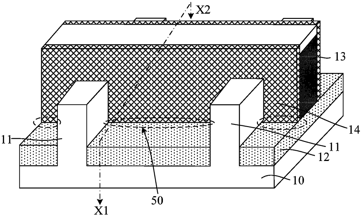
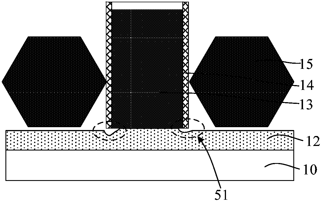
[0015] combined reference figure 1 with figure 2 , showing a structural diagram corresponding to each step in a method for forming a semiconductor structure, figure 1 is a stereogram, figure 2 is based on figure 1 At the location of the isolation structure, the secant line along the direction of fin extension (such as figure 1 The schematic diagram of the cross-sectional structure shown by the X1X2 secant line in .

[0016] refer to figure 1 , providing a base, the base includes a substrate 10 and discrete fins 11 located on the substrate 10; an isolation structure 12 is formed on the substrate 10 exposed by the fins 11, and the isolation structure 12 covers the Part of the sidewall of the fin 11, and the top of the isolation structure 12 is lower than the top of the fin 11; after the isolation stru...


PUM


Abstract

The invention relates to a semiconductor structure and a formation method thereof. The method comprises steps that a substrate and separate fins on the substrate are provided; an isolation structure partially covering side walls of the fin portions is formed on the substrate; after forming the isolation structure, the pseudo gate structure crossing the fin portions and covering a part of top portions of the fin portions and side wall surfaces is formed; sidewalls are formed on the side walls of the pseudo gate structure; after forming the sidewalls, grooves are formed in the fins on both sidesof the pseudo gate structure; a doped epitaxial layer is formed in the grooves; after forming the doped epitaxial layer, an interlayer dielectric layer is formed on the isolation structure not covered by the pseudo gate structure, and the top portion of the pseudo gate structure is not covered by the interlayer dielectric layer; the pseudo gate structure is removed, and an opening is formed in the interlayer dielectric layer; a barrier layer is formed at the bottom of the opening; the barrier layer in the opening is removed; after removing the barrier layer, a metal layer is used for fillingthe opening to form the metal gate structure. The method is advantaged in that through the barrier layer, the doped epitaxial layer and the meal layer are isolated, and thereby the probability of bridging the metal gate structure and the doped epitaxial layer is reduced.

Description

technical field [0001] The invention relates to the field of semiconductors, in particular to a semiconductor structure and a forming method thereof. Background technique [0002] In semiconductor manufacturing, with the development trend of VLSI, the feature size of integrated circuits continues to decrease. In order to accommodate the reduction in feature size, the channel length of MOSFETs has also been shortened accordingly. However, as the channel length of the device is shortened, the distance between the source and the drain of the device is also shortened, so the control ability of the gate to the channel becomes worse, and the gate voltage pinches off the channel. The difficulty is also increasing, making the phenomenon of subthreshold leakage (subthreshold leakage), the so-called short-channel effect (SCE: short-channel effects) more likely to occur. [0003] Therefore, in order to better adapt to the reduction of the feature size, the semiconductor process gradu...

Claims


Application Information

Patent Timeline
IPC IPC(8): H01L21/336H01L21/8238H01L29/78H01L27/092
CPCH01L27/0924H01L29/66545H01L29/66795H01L29/785H01L21/823821
Inventor 李勇
Owner SEMICON MFG INT (SHANGHAI) CORP
Why Eureka
Try Eureka