Wafer-level chip structure, multi-chip stacking interconnection structure and preparation method

A wafer-level chip and chip structure technology, which is applied in semiconductor/solid-state device manufacturing, semiconductor/solid-state device parts, semiconductor devices, etc., can solve problems such as the impact of signal transmission quality, improve signal distortion, and improve signal distortion , Improve the effect of bridging problems

Active Publication Date: 2020-08-18
SHANGHAI XIANFANG SEMICON CO LTD +1
View PDF8 Cites 4 Cited by
  • Summary
  • Abstract
  • Description
  • Claims
  • Application Information

AI Technical Summary

Problems solved by technology

[0004] Therefore, the present invention provides a wafer-level chip structure, a multi-chip stacked interconnection structure and a preparation method, which overcome the problem in the prior art that the impedance of the signal transmission path is constantly changing during 3D chip packaging or wafer-level packaging. Defects that cause a noticeable impact on signal transmission quality

Method used


Image

  • Wafer-level chip structure, multi-chip stacking interconnection structure and preparation method
  • Wafer-level chip structure, multi-chip stacking interconnection structure and preparation method
  • Wafer-level chip structure, multi-chip stacking interconnection structure and preparation method

Examples


Embodiment 1

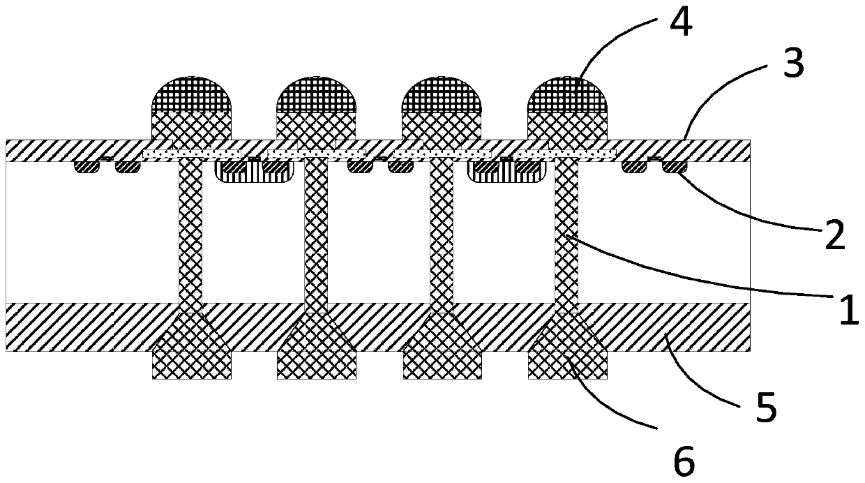
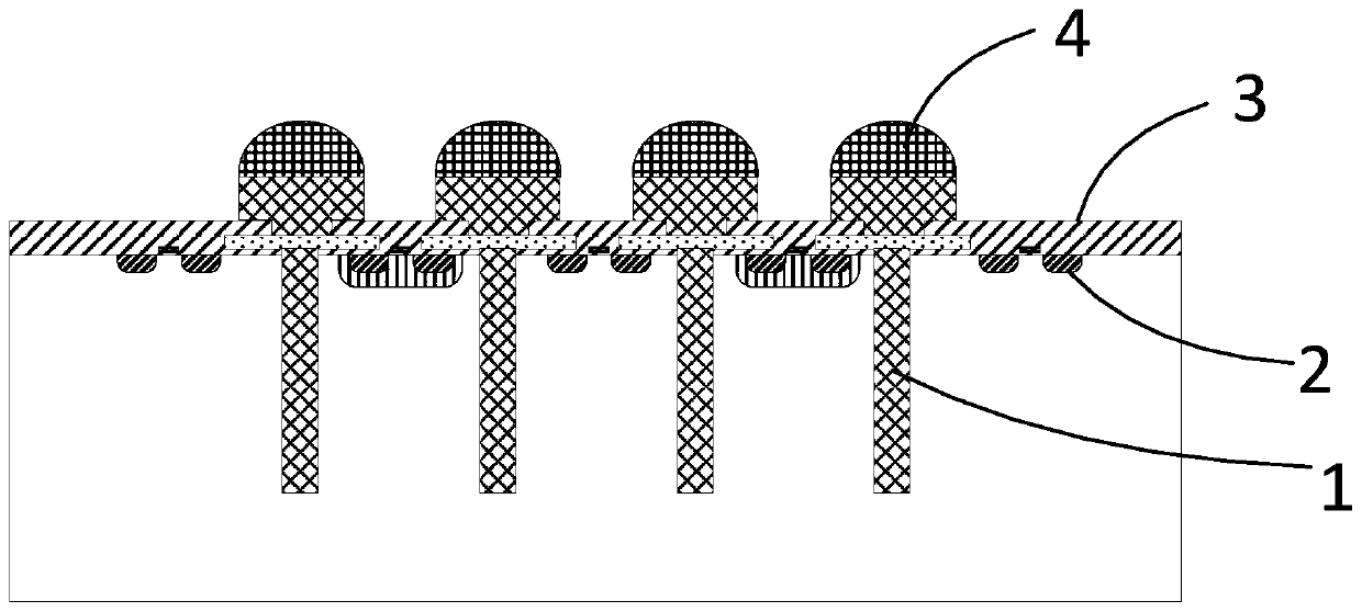
[0052] Embodiments of the present invention provide a wafer-level chip structure, such as figure 1 As shown, it includes: through-silicon via 1 through the wafer, its first surface includes: active region 2, multi-layer redistribution line layer 3 and bump 4, its second surface includes: insulating dielectric layer 5, and A frustum-conical transition structure 6 connected by through-silicon vias.

[0053] In the embodiment of the present invention, the material filled in the TSV 1 can be copper, the bump 4 can be a solder ball, the opening diameter of one end of the frustum-conical transition structure 6 is determined according to the size of the connected TSV, and the opening diameter of the other end is determined according to Bonding bump size determination. The frustoconical transition structure is based on SF 6 / CF 4 / CHF 3 / O 2 / Ar and other process gas inductively coupled plasma etching process, the height is about 2 ~ 6um (SiO 2 Deposition thickness and film stre...

Embodiment 2

[0062] An embodiment of the present invention provides a wafer-level multi-chip stacking interconnection structure, such as Figure 7 As shown, it includes: a chip bonder 7, a substrate 8 and a lead terminal 9, the chip bonder 7 is transferred to the first surface of the substrate 8, and the lead terminal 9 is formed on the second surface of the substrate, wherein,

[0063] The chip bonding body 7 includes a plurality of single wafer-level chips arranged in a stack, and the multiple single wafer-level chips are directly connected through a bonding layer. The single wafer-level chips include: a first chip structure 11, A second chip structure 12 and at least one third chip structure 13, the first chip structure 11 and the second chip structure 12 are respectively located at both ends of the chip bonding body 7, the at least one third chip structure 13, Located between the first chip structure 11 and the second chip structure 12; the third chip structure 13 is the wafer-level ch...


PUM


Abstract

The invention discloses a wafer-level chip structure, a multi-chip stacking interconnection structure and a preparation method. The wafer-level chip structure comprises through silicon vias penetrating through a wafer; a first surface of the wafer comprises an active region, a plurality of redistribution line layers and bumps; and a second surface of the wafer comprises an insulating dielectric layer and frustum transition structures connected with the through silicon vias. According to the embodiment of the invention, the frustum-shaped impedance transition structures are introduced between TSV exposed areas on the back surface of the wafer and the UBM to make impedance matching between the TSV and the UBM realized, so that the problem of signal distortion caused by sudden change of impedance is solved; and compared with a traditional scheme, in order to achieve the frustum-shaped transition structures of the scheme, the number of photomasks is not increased, only one photoetching process and one reactive ion etching process are added on the basis of the original process, so that the process flow is not complex.

Description

technical field [0001] The invention relates to the technical field of semiconductor packaging, in particular to a wafer-level chip structure, a multi-chip stacking interconnection structure and a preparation method. Background technique [0002] In recent years, in the application of 3D stacking of multi-layer chips using TSV (Through Silicon Via) and micro-bumps, the electrical signal transmission path between the upper and lower stacked chip layers is: the RDL of the upper chip layer, the upper chip layer Buried vertical interconnection (TSV), bonding micro-bumps between the upper and lower chip layers, UBM of the lower layer chip, embedded vertical interconnection (TSV) of the lower layer chip and RDL of the lower chip layer. On the signal transmission path, the impedance of the transmission line is constantly changing, and the change and fluctuation of the impedance will have a significant impact on the quality of the signal transmission, such as the reduction of the ey...

Claims


Application Information

Patent Timeline
Patent Type & Authority Applications(China)
IPC IPC(8): H01L23/48H01L23/485H01L21/768H01L21/60
CPCH01L23/481H01L23/4824H01L24/08H01L24/03H01L21/76898H01L24/82H01L2224/0231H01L2224/02331H01L2224/02381H01L2224/08146H01L2224/16225H01L2224/73204H01L2224/16145H01L25/0657H01L2225/06513H01L2225/06541H01L2225/06586H01L2225/06517H01L25/50H01L24/16H01L24/13H01L21/561H01L21/563H01L21/565H01L23/3135H01L23/64H01L24/32H01L24/73H01L24/83H01L24/96H01L24/97H01L2224/1601H01L2224/16148H01L2224/3201H01L2224/32145H01L2224/83203H01L2224/96H01L2224/97H01L2225/06524H01L2225/06544H01L2924/1436H01L2924/30111H01L2924/3841
Inventor 严阳阳曹立强孙鹏陈天放戴风伟
Owner SHANGHAI XIANFANG SEMICON CO LTD
Why Eureka
Try Eureka