Supercharge Your Innovation With Domain-Expert AI Agents!

PCB inner line graph transfer process

A technology of graphic transfer and inner layer circuit, which is applied in the direction of circuit cover, printed circuit, printed circuit manufacturing, etc., can solve the problems of wasting electricity and time, high cost, and environmental protection, so as to improve the process ability, improve the manufacturing ability, work high efficiency effect

Active Publication Date: 2018-09-14
广东诚展科技股份有限公司
View PDF3 Cites 8 Cited by
  • Summary
  • Abstract
  • Description
  • Claims
  • Application Information

AI Technical Summary

Problems solved by technology

[0003] 1. When the photosensitive wet film method is rolled or printed, it needs to be baked at 110°C for about 10 minutes. It is easy to stick to film (film), and the photosensitive wet film process wastes a lot of electricity and time, and the discharge of solvents will cause certain environmental pollution protection, which is not environmentally friendly
[0004] 2. The dry film of the photosensitive dry film method is not easy to achieve a small film thickness. Since the dry film itself has a layer of PE film, and a protective film of the film itself is added during exposure, the resolution is not high and the cost is high; The highest level in the industry is 2 / 2mil, which cannot meet the demand for high-precision interconnection HDI (High Density Interconnector, high-density interconnection) products

Method used


Image

  • PCB inner line graph transfer process
  • PCB inner line graph transfer process

Examples


Embodiment Construction

[0022] It should be noted that, in the case of no conflict, the embodiments of the present invention and the features in the embodiments can be combined with each other. The technical solutions of the present invention will be further described below in conjunction with the accompanying drawings, and the present invention is not limited to the following specific embodiments.

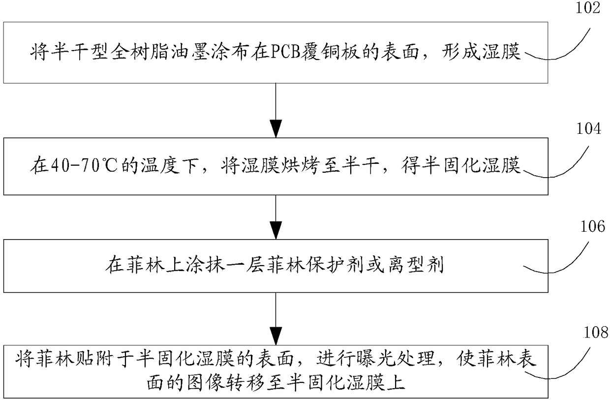
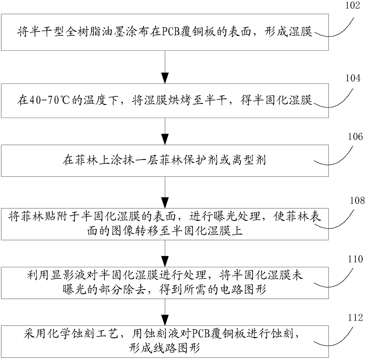
[0023] The invention provides a PCB inner layer circuit graphics transfer process, such as figure 1 shown, including the following steps.

[0024] Step 102, coating the semi-dry full resin ink on the surface of the PCB copper clad board to form a wet film. This step may also be referred to as an ink coating step.

[0025] Step 104, at a temperature of 40-70° C., bake the wet film until it is semi-dry to obtain a semi-cured wet film. This step can also be called a pre-baking step.

[0026] Step 106, apply a layer of film protection agent or release agent on the film. This step can also be referred to...


PUM

PropertyMeasurementUnit
Hardnessaaaaaaaaaa

Abstract

The invention discloses a PCB inner line graph transfer process comprising the following steps: the ink coating step: the semi-dry all-resin ink is coated on the surface of a PCB copper-clad plate soas to form a wet film; the pre-baking step: the wet film is baked to the semi-dry state under the temperature of 40-70 DEG C so as to obtain the semi-cured wet film; the film processing step: a layerof film protectant or release agent is coated on the film; and the exposure step: the film is attached to the surface of the semi-cured wet film to perform exposure processing so that the image on thesurface of the film is enabled to be transferred to the semi-cured wet film. According to the PCB inner line graph transfer process, the working efficiency is high, the product preparation period canbe shortened, the manufacturing process capacity can be enhanced, the line of minimum linewidth / line space=1 / 1mil can be analyzed and manufactured by the process, the precise line manufacturing capacity of the PCB (printed circuit board) can be enhanced, production of the high-precision interconnection HDI product at the highest level in the world can be met, and energy conservation, emission reduction and consumption reduction can be realized and thus the process is more environment-friendly.

Description

technical field [0001] The invention relates to a PCB inner layer circuit pattern transfer process. Background technique [0002] At present, in the pattern transfer process of PCB (Printed Circuit Board, circuit board) inner layer circuit production, the industry uses photosensitive wet film or photosensitive dry film for pattern transfer, because both methods have the following defects: [0003] 1. When the photosensitive wet film method is rolled or printed, it needs to be baked at 110°C for about 10 minutes. It is easy to stick to film (film), and the photosensitive wet film process wastes a lot of electricity and time, and the discharge of solvents will cause certain environmental pollution and protection, which is not environmentally friendly. [0004] 2. The dry film of the photosensitive dry film method is not easy to achieve a small film thickness. Since the dry film itself has a layer of PE film, and a protective film of the film itself is added during exposure, t...

Claims


Application Information

Patent Timeline
IPC IPC(8): H05K3/00
CPCH05K3/0082H05K2203/052
Inventor 杨仁鸿
Owner 广东诚展科技股份有限公司
Features
  • R&D
  • Intellectual Property
  • Life Sciences
  • Materials
  • Tech Scout
  • Unparalleled Data Quality
  • Higher Quality Content
  • 60% Fewer Hallucinations
Learn More