
TFT array substrate and manufacturing method thereof

A technology of an array substrate and a manufacturing method, which is applied in the field of TFT array substrate and its manufacturing, can solve the problems of long production time, high production cost, application limitation and the like, and achieve the effects of saving production time, saving production cost and improving electrical performance.

Active Publication Date: 2020-11-24
TCL CHINA STAR OPTOELECTRONICS TECH CO LTD
View PDF6 Cites 0 Cited by
  • Summary
  • Abstract
  • Description
  • Claims
  • Application Information

AI Technical Summary

Problems solved by technology

However, the traditional single-gate device structure is limited in its application in large-area resolutions such as AMOLED screens and AMLCDs due to its low mobility.
[0005] In order to meet the requirements of large area and high resolution, a double-gate device structure is usually used to improve mobility. Compared with a single-gate device structure, the double-gate device structure is not in the same plane because its top gate and bottom gate are not in the same plane. An extra photomask will be used during production, resulting in high production cost and long production time

Method used


Image

  • TFT array substrate and manufacturing method thereof
  • TFT array substrate and manufacturing method thereof
  • TFT array substrate and manufacturing method thereof

Examples


Embodiment Construction

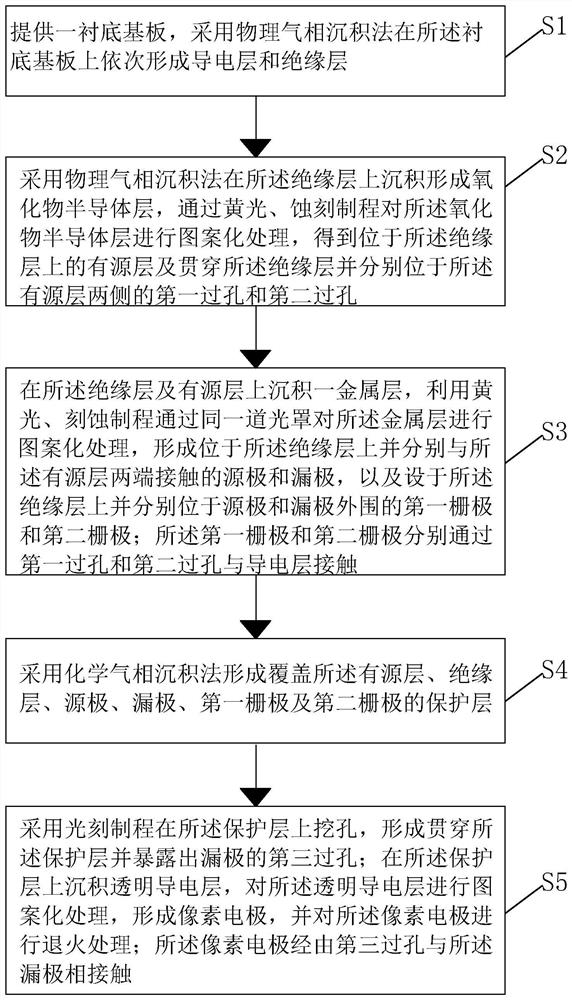
[0042] In order to further illustrate the technical means adopted by the present invention and its effects, the following describes in detail in conjunction with preferred embodiments of the present invention and accompanying drawings.

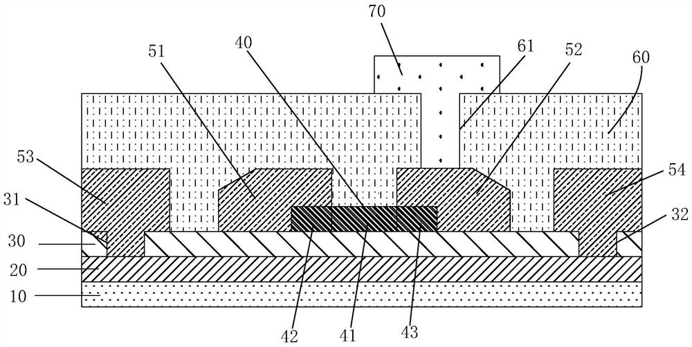
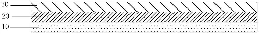
[0043] see figure 1, the present invention provides a TFT array substrate, including a base substrate 10, a conductive layer 20 disposed on the base substrate 10, an insulating layer 30 disposed on the conductive layer 20, and an insulating layer 30 disposed on the insulating layer 30. The active layer 40 on the upper surface, the source electrode 51 and the drain electrode 52 arranged on the insulating layer 30 and in contact with both ends of the active layer 40 respectively, and the source electrode 51 arranged on the insulating layer 30 and respectively located at the source electrode 51 and the first gate 53 and the second gate 54 on the periphery of the drain 52;

[0044] The first gate 53 and the second gate 54 are respectively in cont...


PUM

PropertyMeasurementUnit
widthaaaaaaaaaa

Abstract

The invention provides a TFT array substrate and a manufacturing method thereof. The source, drain, first gate, and second gate of the TFT array substrate are all formed on the insulating layer, that is, on the same plane, so the source, drain, and first gate can be fabricated at the same time using the same photomask and the second gate to save production cost and production time, and an equivalent capacitance will be formed between the first gate and the source and between the second gate and the drain, by adjusting the first gate and the source The distance between the electrodes and the distance between the second gate and the drain can effectively regulate the threshold voltage and sub-threshold swing of the TFT device appropriately, and improve the electrical performance of the TFT device.

Description

technical field [0001] The invention relates to the field of display technology, in particular to a TFT array substrate and a manufacturing method thereof. Background technique [0002] With the development of display technology, liquid crystal displays (Liquid Crystal Display, LCD) and other flat display devices are widely used in mobile phones, televisions, personal Various consumer electronic products such as digital assistants, digital cameras, notebook computers, and desktop computers have become the mainstream of display devices. [0003] Most of the liquid crystal display devices currently on the market are backlight liquid crystal displays, which include a liquid crystal display panel and a backlight module. The working principle of the liquid crystal display panel is to place liquid crystal molecules between two parallel glass substrates. There are many vertical and horizontal small wires between the two glass substrates. The direction of the liquid crystal molecul...

Claims


Application Information

Patent Timeline
Patent Type & Authority Patents(China)
IPC IPC(8): H01L27/12H01L27/32H01L21/77
CPCH01L27/1225H01L27/124H01L27/1288H10K59/131
Inventor 曹威
Owner TCL CHINA STAR OPTOELECTRONICS TECH CO LTD
Learn More