Enhanced GaN transistor and preparation method thereof

A gallium nitride and transistor technology, applied in semiconductor/solid-state device manufacturing, semiconductor devices, electrical components, etc., can solve problems such as etching damage, and achieve the effect of increasing gate threshold voltage and reducing gate leakage current

Inactive Publication Date: 2018-09-28
珠海镓未来科技有限公司
View PDF1 Cites 2 Cited by
  • Summary
  • Abstract
  • Description
  • Claims
  • Application Information

AI Technical Summary

Problems solved by technology

One is to etch the gate trench to reduce the two-dimensional electron gas density in the conductive channel by reducing the thickness of the barrier layer, but this method will introduce additional etching damage, and this method can only reduce the gallium nitride The threshold voltage of the device is raised to around 1V

Method used


Image

  • Enhanced GaN transistor and preparation method thereof
  • Enhanced GaN transistor and preparation method thereof
  • Enhanced GaN transistor and preparation method thereof

Examples


Embodiment Construction

[0039] The present invention will be further described in detail below in conjunction with the accompanying drawings and embodiments. It should be understood that the specific embodiments described here are only used to explain the present invention, but not to limit the present invention. In addition, it should be noted that, for the convenience of description, only some structures related to the present invention are shown in the drawings but not all structures.

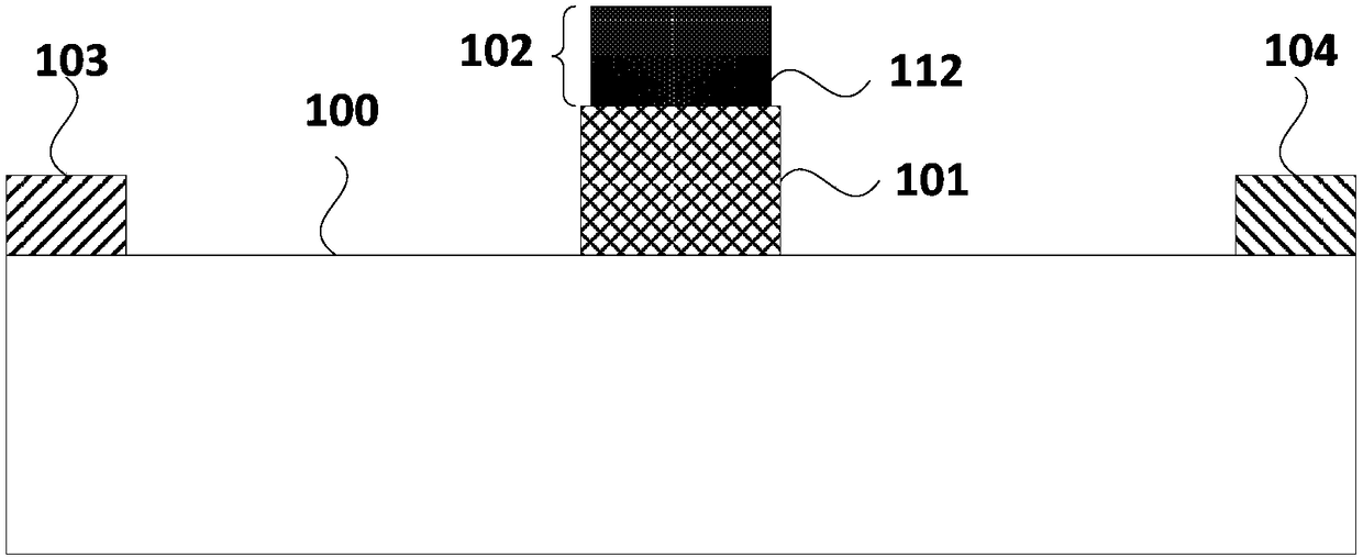
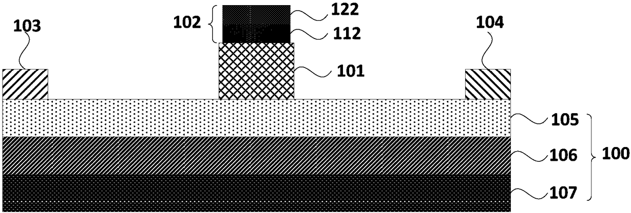
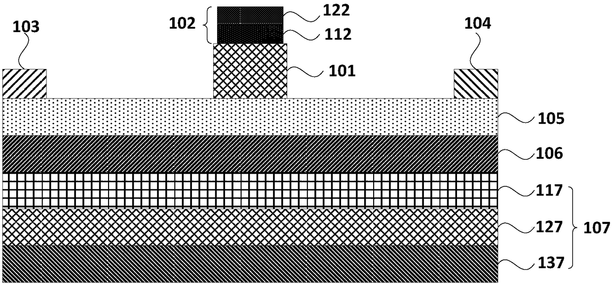
[0040] figure 1 It is a schematic structural diagram of an enhancement mode gallium nitride transistor provided by an embodiment of the present invention. Optionally, refer to figure 1 , the enhancement mode gallium nitride transistor includes: a substrate 100, the substrate 100 includes a source region and a drain region, and a gate region between the source region and the drain region; a gallium nitride modulation gate 101 is located in the gate region, and the gallium nitride modulation The gate 101 includes ...


PUM


Abstract

The invention discloses an enhanced GaN transistor and a preparation method thereof. The transistor comprises a substrate, wherein the substrate comprises a source region and a drain region, and a gate region located between the source region and the drain region; a GaN modulation gate located at the gate region, wherein the GaN modulation gate comprises a GaN material doped with P-type ions; a source electrode and a drain electrode, wherein the source electrode is located at the source region and the drain electrode is located at the drain region; and a gate metal layer, which is located on the surface, away from the substrate, of the GaN modulation gate, wherein the grid electrode metal layer at least comprises a lanthanide metal layer, and the lanthanide metal layer is in contact with the GaN modulation grid. According to the enhanced GaN transistor provided by the embodiment of the invention, the lanthanide metal layer is arranged on one side, far away from the substrate, of the GaN modulation grid, and the lanthanide metal layer is enabled to be in contact with the GaN modulation gate; and when the enhanced GaN transistor works, a higher voltage is required to conduct a channel between the source electrode and the drain electrode, thereby improving the gate threshold voltage of the enhanced GaN transistor and reducing the gate leakage current.

Description

technical field [0001] Embodiments of the present invention relate to the technical field of preparation of broadband power devices, and in particular to an enhancement mode gallium nitride transistor and a preparation method thereof. Background technique [0002] Gallium nitride is a semiconductor material with the characteristics of large band gap, high electron saturation drift velocity, high breakdown field strength and good thermal conductivity, and has become an important third-generation semiconductor material. In the field of electronic devices, compared with silicon materials, gallium nitride materials are more suitable for manufacturing high-temperature, high-frequency, high-voltage and high-power devices, and have good application prospects. [0003] In order to obtain high-temperature, high-frequency, high-voltage and high-power gallium nitride devices, it is first necessary to prepare gallium nitride high electron mobility transistors (Gallium Nitride High Elect...

Claims


Application Information

Patent Timeline
Patent Type & Authority Applications(China)
IPC IPC(8): H01L29/41H01L21/336H01L29/778
CPCH01L29/41H01L29/66462H01L29/778
Inventor 于洪宇章剑
Owner 珠海镓未来科技有限公司
Why Eureka
Try Eureka