Longitudinally-conductive GaN (gallium nitride) normally-closed MISFET (metal integrated semiconductor field effect transistor) device and manufacturing method thereof

A manufacturing method and normally-off technology, which is applied in semiconductor/solid-state device manufacturing, semiconductor devices, electrical components, etc., can solve the problem of reduced channel electron mobility, increased device on-resistance, and lattice damage at the edge of the groove. and other problems to achieve the effect of improving mobility, reducing on-resistance, and improving device reliability

Active Publication Date: 2012-01-25
SHANGHAI XINYUANJI SEMICON TECH
View PDF2 Cites 24 Cited by
  • Summary
  • Abstract
  • Description
  • Claims
  • Application Information

AI Technical Summary

Problems solved by technology

[0007] From the above reports, the on-resistance of GaN-based recessed gate vertical conduction normally-off devices is still relatively high, and the electron mobility in the channel is relatively low, which is mainly due to the formation of grooves in the heterostructure by ICP etching. During the process, damage to the lattice at the edge of the groove
In the working engineering of the device, the edge of the groove is used as a conductive channel. Due to the influence of the damaged lattice, the on-resistance of the device becomes larger and the electron mobility of the channel decreases.

Method used


Image

  • Longitudinally-conductive GaN (gallium nitride) normally-closed MISFET (metal integrated semiconductor field effect transistor) device and manufacturing method thereof
  • Longitudinally-conductive GaN (gallium nitride) normally-closed MISFET (metal integrated semiconductor field effect transistor) device and manufacturing method thereof
  • Longitudinally-conductive GaN (gallium nitride) normally-closed MISFET (metal integrated semiconductor field effect transistor) device and manufacturing method thereof

Examples


Embodiment 1

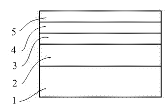
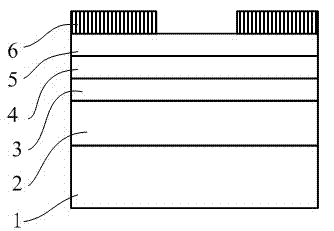
[0041] like Figure 10 Shown is a schematic diagram of the device structure of this embodiment, including a gate 11, a source 9, a drain 10, an insulating layer 8, a conductive GaN substrate 1, an n-type GaN layer 2, an electron blocking layer 3, and a non-doped GaN layer 4 and the heterostructure barrier layer 5, dry etching to form grooves, secondary growth of the p-type GaN layer to realize the gate conductive channel 7, the surface of the channel 7 and the heterostructure barrier layer 5 covering the insulating layer 8 , the gate 11 covers the channel 7 on the insulating layer, and the insulating layer 8 and SiO are etched 2 A source region is formed at both ends of the mask, and ohmic metal is evaporated on the source region to form a source 5 in contact with the heterostructure barrier layer 5, and the drain 10 is placed on the back of the conductive GaN substrate. In this embodiment, the conductive GaN substrate 1 is a heavily doped GaN substrate, and the n-type GaN la...

Embodiment 2

[0054] like Figure 11 Shown is a schematic diagram of the device structure of this embodiment, which is similar to that of Embodiment 1, the only difference being that an AlN layer 12 with a thickness of 5-50 nm is grown before the non-doped GaN layer 4 is grown on the electron blocking layer 3 . Because in the growth of the electron blocking layer 3, p-type doping is carried out in order to make this layer form a high-resistance blocking layer of electrons, impurities may diffuse into the non-doped GaN layer 4 on the upper layer during the growth process, affecting device performance. Therefore, the introduction of a thin layer of AlN layer 12 will effectively block the diffusion of these impurities into the non-doped GaN layer 4 .

Embodiment 3

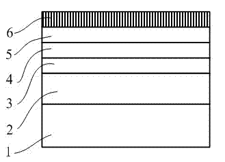
[0056] like Figure 12 Shown is a schematic diagram of the device structure of this embodiment, which is similar to the structure of Embodiment 1, the only difference is that the mask layer 6 is not removed after the groove is etched in the gate region, and the subsequent process steps are directly carried out. The purpose of doing this is to reduce the steps of removing the mask layer 6 and simplify the process flow, and at the same time, the mask layer 6 can be used as a passivation layer.


PUM


Abstract

The invention discloses a longitudinally-conductive GaN (gallium nitride) normally-closed MISFET (metal integrated semiconductor field effect transistor) device and a manufacturing method thereof. The device successively comprises a substrate (1), an n-type GaN layer (2), an electronic barrier layer (3), a non-doped GaN layer (4) and a heterostructure potential barrier layer (5) from bottom to top, wherein a groove is etched in the n-type GaN layer from the surface of the heterostructure potential barrier layer; a p-type GaN layer is formed on the groove by secondary growth so as to realize a grid conducting channel (7); two ends of the heterostructure potential barrier layer form source electrodes (9); an insulating layer (8) is covered on the grid conducting channel and the exposed surface of the heterostructure potential barrier layer; a grid electrode (11) is covered at a channel position on the insulating layer; and drain electrodes (10) are covered on the underside of the substrate. In the invention, a two-dimensional electron gas heterostructure with high concentration is taken as an access area, thus effectively reducing the on resistance; and the thin p-type GaN layer is formed in the etching groove by secondary growth, thus being easy to improve the threshold voltage and channel mobility of the longitudinally-conductive normally-closed MISFET.

Description

technical field [0001] The invention relates to the field of semiconductor devices, in particular to a vertically conducting GaN normally-off MISFET device and a manufacturing method thereof. Background technique [0002] Compared with Si materials, GaN semiconductor materials are more suitable for making high-power Power switching devices with large capacity and high switching speed are ideal substitutes for the next generation of power switching devices. [0003] The GaN material has a strong polarization effect, and the interface of the AlGaN / GaN heterojunction grown in the polarization direction forms a 10 13 cm -2 The two-dimensional electron gas (2DEG) with high concentration and high electron mobility makes AlGaN / GaN heterojunction field effect transistors (HFETs) have extremely low on-resistance, which is very suitable for making power switching devices. Therefore, it is an important subject to realize the practical goal of GaN power switching devices to prepare h...

Claims


Application Information

Patent Timeline
Patent Type & Authority Applications(China)
IPC IPC(8): H01L29/778H01L29/78H01L29/06H01L21/336
Inventor 刘扬杨帆张佰君
Owner SHANGHAI XINYUANJI SEMICON TECH
Why Eureka
Try Eureka