Semiconductor device and method for manufacturing semiconductor device

a semiconductor and semiconductor technology, applied in the direction of semiconductor devices, electrical devices, transistors, etc., can solve the problems of reducing affecting the gate control, and limiting the film thickness of the gate insulator, so as to reduce the impurity concentration, increase the gate threshold voltage, and increase the diffusion coefficient

Active Publication Date: 2014-04-24
FUJI ELECTRIC CO LTD
View PDF10 Cites 3 Cited by
  • Summary
  • Abstract
  • Description
  • Claims
  • Application Information

AI Technical Summary

Benefits of technology

[0038]According to the invention described above, n-type ionic species having a larger diffusion coefficient than ion species used for forming the n+-type source region are implanted into the opening that is formed between the insulator or the gate electrode and the resist mask such that the surface of the p-type well region is exposed, and then the p-type well region and the n-type source region are subjected to annealing simultaneously to diffuse heat therein. A MOS semiconductor device with a thick gate insulator can be obtained by reducing the impurity concentration in the vicinity of the surface of the joint between p-type well region and the n+-type source region without increasing the gate threshold voltage. Alternatively, the gate threshold voltage is reduced while keeping the film thickness of the gate insulator constant. As a result, the effects of the present invention can be achieved.
[0039]In the semiconductor device and the method for manufacturing the same according to the present invention, a semiconductor device with a thick gate insulator can be produced without increasing a gate threshold voltage. Because the intensity of an electric field applied to the gate insulator decreases when the gate insulator is made thick, the reliability of the gate insulator can be improved, thereby enhancing the gate breakdown withstand capability. In addition, providing a thick gate insulator to the semiconductor device can reduce the gate capacity and hence switching losses.

Problems solved by technology

However, the risk in such a relationship is that conduction of a parasitic transistor is made easily during the ON state of the semiconductor device due to the reduced impurity concentration in the channel forming region, resulting in not being able to control the gate.
Consequently, a depletion layer easily expands in the p-type well region during the OFF state of the semiconductor device, which can result in damaging the semiconductor device by punch-through.
Although increasing the film thickness of the gate insulator increases a gate threshold voltage as described above, there is a limit to increasing the film thickness of the gate insulator.
However, the impurity concentration in the surface of the p-type well region is closely related to the withstand voltage and on-resistance of the semiconductor device, there is no choice but setting the impurity concentration within a range not affecting the withstand voltage and on-resistance negatively.
Another problem with Patent Document 5 is that reducing the impurity concentration in the p-type well region allows a depletion layer to spread, consequently causes a short channel effect, and enables operation of a parasitic bipolar transistor.
In addition, providing a thick gate insulator to the semiconductor device can reduce the gate capacity and hence switching losses.

Method used


Image

  • Semiconductor device and method for manufacturing semiconductor device
  • Semiconductor device and method for manufacturing semiconductor device
  • Semiconductor device and method for manufacturing semiconductor device

Examples


embodiment 1

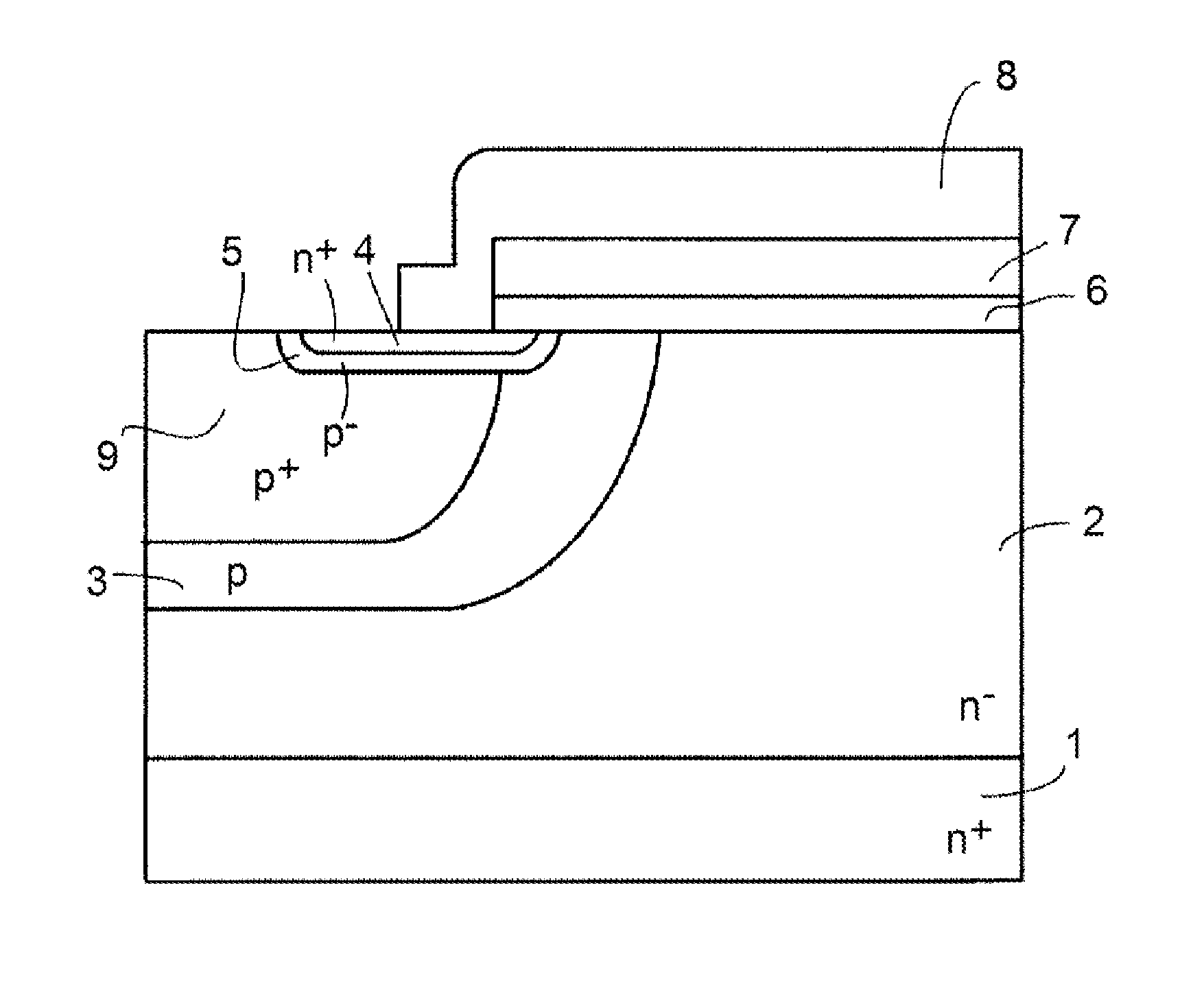
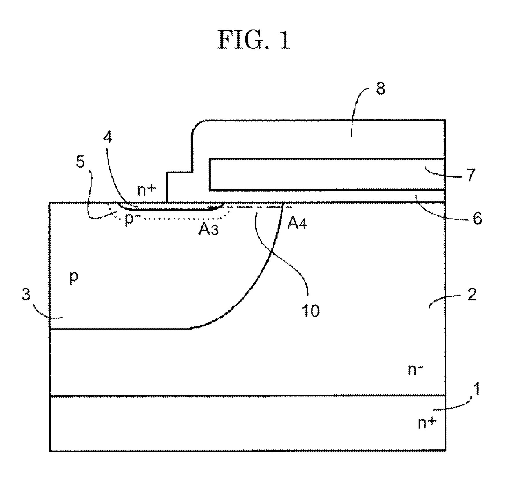
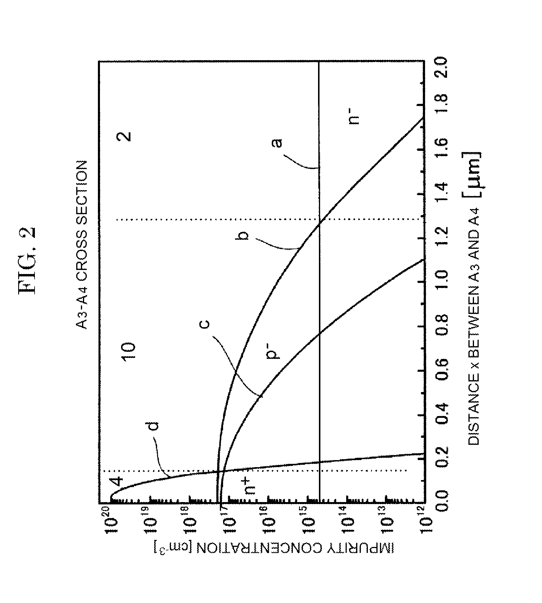
[0083]A semiconductor device according to Embodiment 1 of the present invention is now described with a power MOSFET, one of the MOS-type semiconductor devices, as an example. FIG. 1 is a cross-sectional diagram showing substantial parts of a surface MOS structure of the MOSFET according to Embodiment 1 of the present invention. A surface layer of the front surface of a semiconductor substrate corresponding to an n− layer 2 is selectively provided with a p-type well region 3. Inside the p-type well region 3 are an n+-type source region 4 and a p− region 5 selectively. The n+-type source region 4 is exposed on the front surface of the substrate. The p− region 5 is provided between the n+-type source region 4 and the p-type well region 3 and surrounds the n+-type source region 4. Further, a p+ contact region (not shown) is provided on the inside of the p-type well region 3 so as to be in contact with the p− region 5.

[0084]A front surface of a channel forming region 10 sandwiched betwe...

embodiment 2

[0098]Next is described a method for manufacturing a semiconductor device according to Embodiment 2 of the present invention, with reference to an example of manufacturing an re-channel MOSFET. FIGS. 15 to 22 are cross-sectional diagrams of substantial parts of a semiconductor substrate, each showing sequentially the steps of manufacturing a surface MOS structure of the MOSFET according to Embodiment 2 of the present invention. The difference between the method for manufacturing a semiconductor device according to Embodiment 2 and the method for manufacturing a semiconductor device according to Embodiment 1 is that the gate insulator 6 and the gate electrode 7 made of polysilicon are formed prior to forming the p-type well region 3 and the n+-type source region 4. In other words, masking with the gate electrode 7, the p-type well region 3, the n+-type source region 4, and the p− region 5 are formed by self-alignment in Embodiment 2, the p-type well region 3 being disposed where a ch...

embodiment 3

[0104]Next is described a method for manufacturing a semiconductor device according to Embodiment 3 of the present invention, with reference to an example of manufacturing an re-channel MOSFET. FIGS. 39 to 42 are cross-sectional diagrams of substantial parts of a semiconductor substrate, each showing sequentially the steps of manufacturing a surface MOS structure of a MOSFET according to Embodiment 3 of the present invention. The difference between the method for manufacturing a semiconductor device according to Embodiment 3 and the method for manufacturing a semiconductor device according to Embodiment 1 is that different resist masks are used to perform arsenic ion implantation 16 and phosphorus ion implantation 17. Specifically, the width of an n+-type source region 24 is made narrower than the width of a p− region 25 by narrowing the width of the opening between a resist mask and the oxide mask of the field oxide film 11 during the arsenic ion implantation 16 than in phosphorus ...


PUM


Abstract

A MOS semiconductor device has a MOS structure, including a p region that surrounds an n+-type source region and has a net doping concentration lower than a concentration of a p-type impurity in a surface of a p-type well region, and a gate electrode that is provided on top of the surface of the p-type well region sandwiched between the n+-type source region and a surface layer of an n layer, with a gate insulator disposed between the p-type well region and the gate electrode. This configuration can make the gate insulator thicker without increasing a gate threshold voltage, and help improve the reliability of the gate insulator and reduce the gate capacitance.

Description

BACKGROUND[0001]1. Technical Field[0002]The present invention relates to a MOS-type (metal oxide semiconductor) semiconductor device such as an insulated gate field-effect transistor (MOSFET) or insulated gate bipolar transistor (IGBT), and a method for manufacturing the semiconductor device.[0003]2. Background Art[0004]A surface MOS structure of a power MOSFET, one of the conventional general MOS-type semiconductor devices, is now described. FIG. 4 is a cross-sectional diagram showing substantial parts of a surface MOS structure of a conventional MOSFET. FIG. 5 is a characteristic diagram showing a distribution of impurity concentrations in regions disposed along line A1-A2 in FIG. 4, the distribution being obtained when concentration compensation is not performed at a region boundary. FIG. 6 is a characteristic diagram showing a distribution of impurity concentrations in the regions disposed along line A1-A2 of FIG. 4, the distribution being obtained when concentration compensatio...

Claims


Application Information

Patent Timeline
Patent Type & Authority Applications(United States)
IPC IPC(8): H01L29/66H01L21/266H01L29/78
CPCH01L29/66477H01L29/78H01L21/266H01L29/1095H01L29/6634H01L29/7395H01L21/26513H01L29/66712H01L29/7802H01L29/1045H01L29/66333H01L29/063
Inventor TATEMICHI, SHUHEINISHIMURA, TAKEYOSHINIIMURA, YASUSHIINOUE, MASANORI
Owner FUJI ELECTRIC CO LTD
Why Eureka
Try Eureka