Electronic component

a technology of electronic components and components, applied in the field of electronic components, can solve the problems of increasing pd, increasing increasing manufacturing costs, etc., and achieves the effects of suppressing the increase in dc resistance of the coil, reducing the electric resistance value, and reducing the diffusion coefficien

Active Publication Date: 2020-01-21
TDK CORPARATION
View PDF40 Cites 0 Cited by
  • Summary
  • Abstract
  • Description
  • Claims
  • Application Information

AI Technical Summary

Benefits of technology

[0006]In the stacked coil component according to the aspect of the invention, the inner conductor has a lower electric resistance value than the metal included in the protruding portion. Accordingly, it is possible to suppress an increase in DC resistance of the coil in the stacked coil component according to the aspect. The baked electrode layer of the outer electrode serves as a source of a metal which is used for the connection conductor to protrude from the end surface of the element body to the baked electrode layer and to come in contact with the baked electrode layer due to the Kirkendall effect. In the stacked coil component according to the aspect, the protruding portion of the connection conductor includes a metal which has a smaller diffusion coefficient than the metal of the main component included in the outer electrode. That is, the metal of the main component included in the baked electrode layer has a larger diffusion coefficient than the metal included in the protruding portion and diffuses more easily. Accordingly, in the stacked coil component, the protruding portion is formed by causing the metal to diffuse from the baked electrode layer to the connection conductor in a manufacturing process and causing the connection conductor to expand. In this way, since the protruding portion electrically connecting the connection conductor to the baked electrode layer is formed in the stacked coil component, it is possible to satisfactorily secure connectivity between the inner conductor and the outer electrode. As a result, in the stacked coil component, it is possible to achieve improvement in connectivity between the coil and the outer electrode.
[0007]In the aspect, the metal of a main component included in the baked electrode layer is Ag, and the metal included in the protruding portion is Pd. Pd has a smaller diffusion coefficient than Ag. Accordingly, in the stacked coil component according to the aspect, the metal diffuses satisfactorily from the baked electrode layer to the connection conductor in the manufacturing process. Accordingly, in the stacked coil component according to the aspect, since the protruding portion that satisfactorily electrically connects the connection conductor to the baked electrode layer is formed, it is possible to satisfactorily secure connectivity between the inner conductor and the outer electrode. As a result, in the stacked coil component according to the aspect, it is possible to achieve improvement in connectivity between the coil and the outer electrode.
[0008]In the aspect, the outer surface of the element body may be covered with a glass layer, and the protruding portion may be electrically connected to the outer electrode by penetrating the glass layer. In this configuration, the outer surface of the element body is covered with the glass layer. Accordingly, for example, when a plated layer of the outer electrode is formed, it is possible to prevent a plating solution from permeating the element body and to prevent a plating metal from being extracted from the outer surface of the element body.
[0009]According to the aspect of the invention, it is possible to suppress an increase in DC resistance of a coil and to achieve improvement in connection between the coil and an outer electrode.

Problems solved by technology

However, when the inner conductor is formed of an alloy of Ag and Pd, a manufacturing cost increases because Pd is expensive and DC resistance of a coil increases.
On the other hand, when the inner conductor does not include Pd and the inner conductor is formed of Ag, DC resistance of the coil decreases but connection between the inner conductor and an outer electrode may not be satisfactory due to a Kirkendall effect.

Method used


Image

  • Electronic component
  • Electronic component
  • Electronic component

Examples


first embodiment

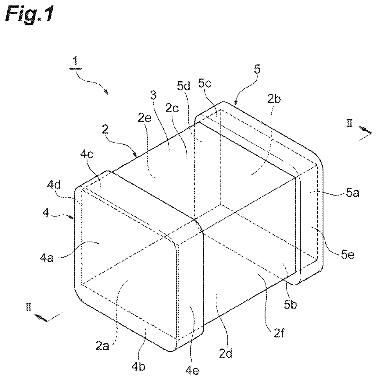
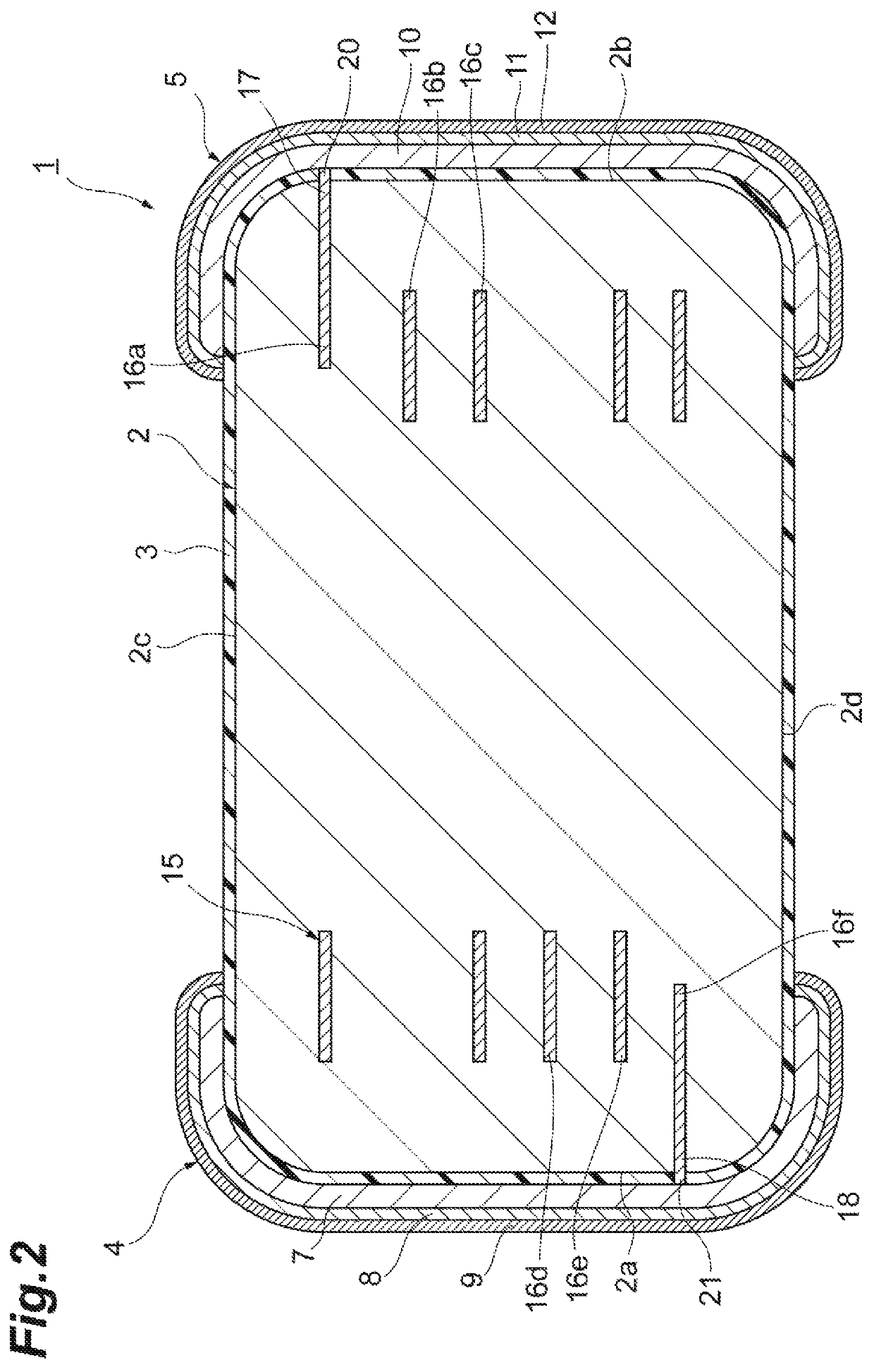
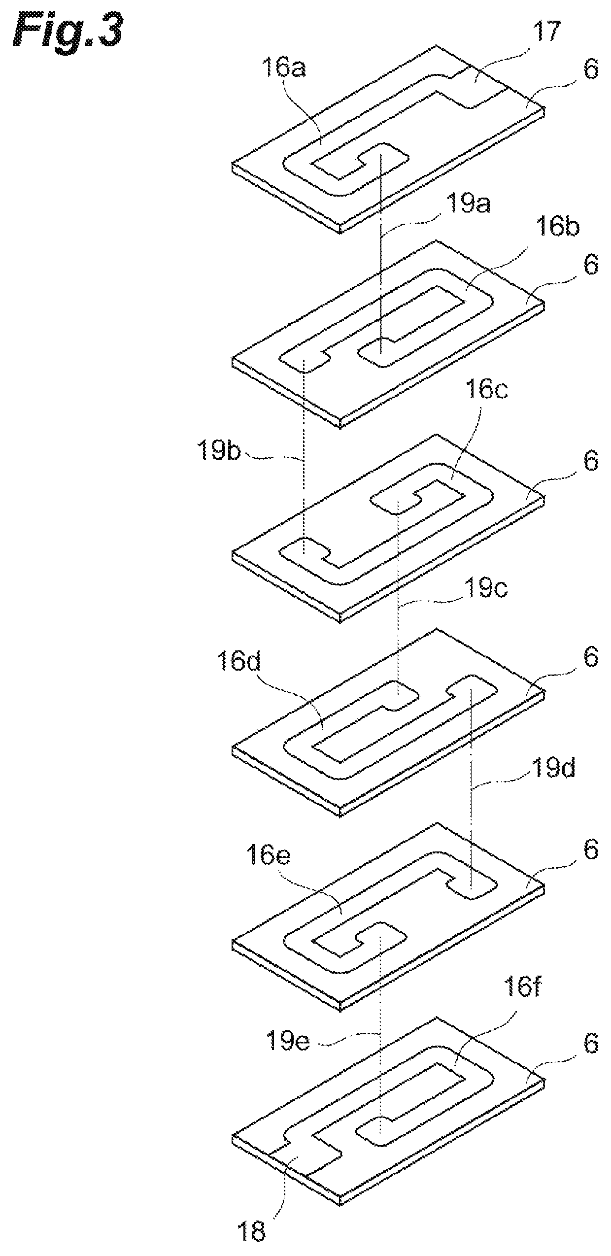
[0025]As illustrated in FIG. 1, a stacked coil component 1 according to a first embodiment includes an element body 2 and a pair of outer electrodes 4 and 5 that are disposed at both ends of the element body 2.

[0026]The element body 2 has a rectangular parallelepiped shape. The element body 2 includes a pair of end surfaces 2a and 2b facing each other, a pair of principal surfaces 2c and 2d facing each other and extending to connect the pair of end surfaces 2a and 2b to each other, and a pair of side surfaces 2e and 2f facing each other and extending to connect the pair of principal surfaces 2c and 2d to each other. The principal surface 2c or the principal surface 2d is defined as a surface facing another electronic device, for example, when the stacked coil component 1 is mounted on another electrode device (for example, a circuit board or an electronic component) which is not illustrated.

[0027]The direction in which the end surfaces 2a and 2b face, the direction in which the prin...

second embodiment

[0055]A second embodiment will be described below. First, the background and summary of the second embodiment will be described.

BACKGROUND

[0056]Japanese Unexamined Patent Publication No. 2004-128448 discloses an electronic component. The electronic component described in Japanese Unexamined Patent Publication No. 2004-128448 includes an element body, an inner conductor that is disposed in the element body, and an outer electrode that is disposed on the outer surface of the element body and is electrically connected to the inner conductor. In the electronic component described in Japanese Unexamined Patent Publication No. 2004-128448, a glass layer is formed on the outer surface of the element body in which the outer electrode is not disposed.

[0057]However, in the convention electronic component, the glass layer is not formed on the outer surface of the element body in which the outer electrode is disposed. Accordingly, when a plated layer is formed in the process of forming the oute...

third embodiment

[0082]A third embodiment will be described below. First, the background and summary of the third embodiment will be described.


PUM

PropertyMeasurementUnit
thicknessaaaaaaaaaa
softening pointaaaaaaaaaa
diffusion coefficientaaaaaaaaaa

Abstract

An electronic component includes: an element body in which a plurality of insulator layers are stacked; a coil in which a plurality of inner conductors installed in the element body are electrically connected to each other; and an outer electrode that is disposed on an outer surface of the element body, is electrically connected to the coil, and includes at least a baked electrode layer. The inner conductor connected to the outer electrode includes a connection conductor that electrically connects the baked electrode layer to the inner conductor. The connection conductor includes a protruding portion that protrudes from the outer surface of the element body to the outer electrode. The protruding portion includes a metal having a smaller diffusion coefficient than a metal of a main component included in the baked electrode layer. The inner conductors have a lower electric resistance value than the metal included in the protruding portion.

Description

BACKGROUND OF THE INVENTIONField of the Invention[0001]The present invention relates to an electronic component.Related Background Art[0002]Japanese Unexamined Patent Publication No. H9-007879 discloses an electronic component. The electronic component described in Japanese Unexamined Patent Publication No. H9-007879 includes an element body, an inner conductor that is disposed in the element body, and an outer electrode that is electrically connected to the inner conductor. In the electronic component described in Japanese Unexamined Patent Publication No. H9-007879, a glass layer is disposed between the element body and the outer electrode and the inner conductor is connected to the outer electrode by penetrating the glass layer.[0003]In a stacked coil component, an inner conductor is generally formed of a conductive material including metals Ag and Pd. However, when the inner conductor is formed of an alloy of Ag and Pd, a manufacturing cost increases because Pd is expensive and ...

Claims


Application Information

Patent Timeline
Patent Type & Authority Patents(United States)
IPC IPC(8): H01F5/00H01F41/12H01F27/32H01F27/29H01F27/28H01F41/04
CPCH01F27/323H01F41/041H01F27/2804H01F27/29H01F41/122H01F2027/2809H01G4/224H01G4/232H01G4/2325H01G4/30H01F17/0013H01F27/292
Inventor SATO, SHINICHITADAKI, YOHEIOIDE, AKIHIKOISHIKAWA, YUMASATO, HIDEKAZUEBINA, KAZUHIROTANOUE, HIROYUKI
Owner TDK CORPARATION
Why Eureka
Try Eureka