

Waveform mapping and gated laser voltage imaging
A technology of gating signals and circuits, which is applied in the directions of optics, measurement electronics, and optical components, and can solve problems such as inefficiency
- Summary
- Abstract
- Description
- Claims
- Application Information
AI Technical Summary
Problems solved by technology
Method used
Image

Examples
Embodiment Construction
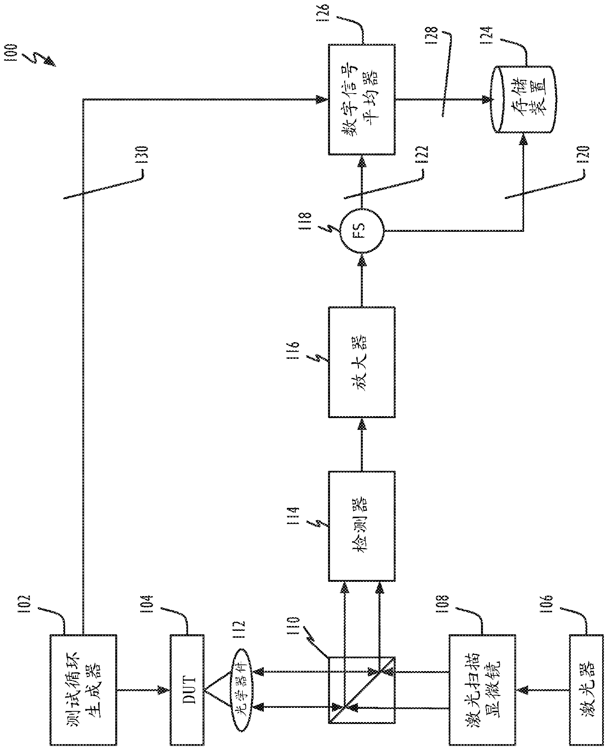
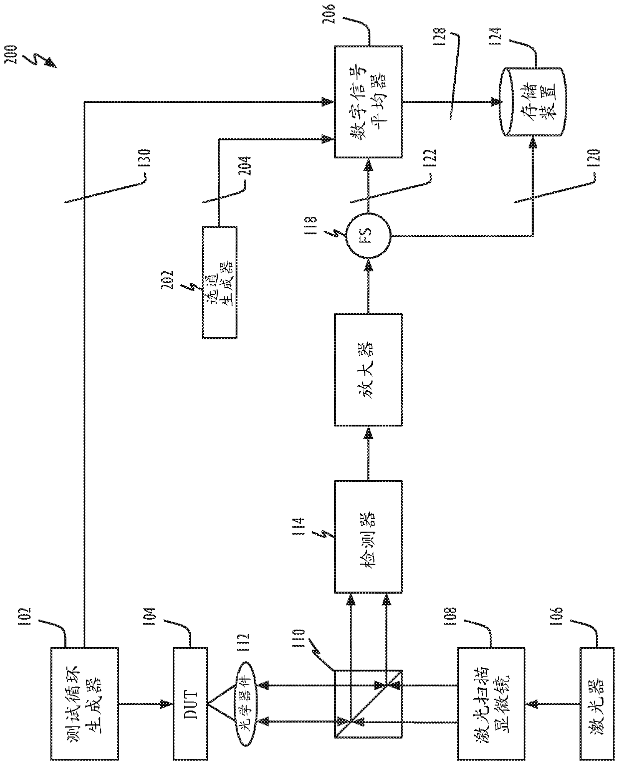
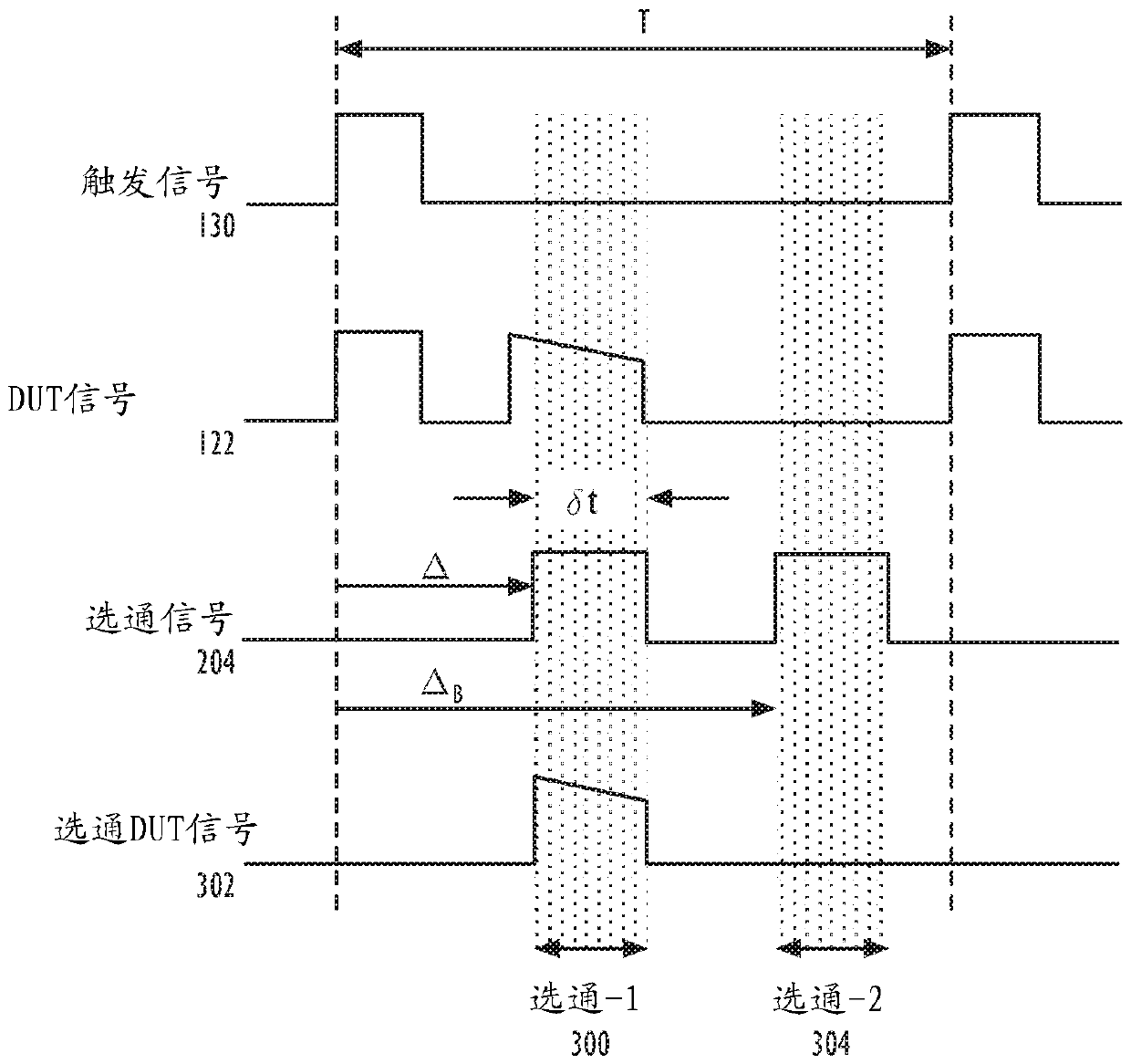
[0019] The present disclosure relates to systems, methods, and computer-readable media for improving integrated circuit (IC) debug operations. Generally, techniques are disclosed for acquiring / recording waveforms across an integrated circuit under test during a single scan of a laser scanning microscope (LSM). More specifically, the techniques disclosed herein allow the response of an integrated circuit to a test signal to be captured at every location across the circuit in real time. The techniques disclosed herein can eliminate the need for most manual probing, which speeds up the debugging process. Furthermore, because acquired waveforms can be automatically correlated to specific pixels in the LSM image, data maps can be created and overlaid onto the LSM image. This map can then highlight any Presence or absence of specified frequencies (for example, using Fourier transform analysis), presence or absence of specific pulses within the test signal (pass / fail data), and / or...
PUM
 Abstract
Description
Claims
Application Information