Laser beam induced phenomena detection

Inactive Publication Date: 2005-05-24
GLOBALFOUNDRIES INC
View PDF3 Cites 24 Cited by
  • Summary
  • Abstract
  • Description
  • Claims
  • Application Information

AI Technical Summary

Benefits of technology

[0009]In accordance with another aspect of the present invention, an apparatus is provided that includes a laser scanning microscope for directing a laser beam at a circuit structure and a source for biasing and thereby establishing a power condition in the circuit structure. The source has a voltage source and a series-connected inductor. The series-connected inductor is operable to slow the responsiveness of the source to chances in the power condition of the cir

Problems solved by technology

However, integrated circuits, such as microprocessors, require high current biasing that is often beyond the specification limits of commercially available current sources.
Moreover, the detection of current change is difficult to implement in general.
Anoth

Method used


Image

  • Laser beam induced phenomena detection
  • Laser beam induced phenomena detection
  • Laser beam induced phenomena detection

Examples


Embodiment Construction

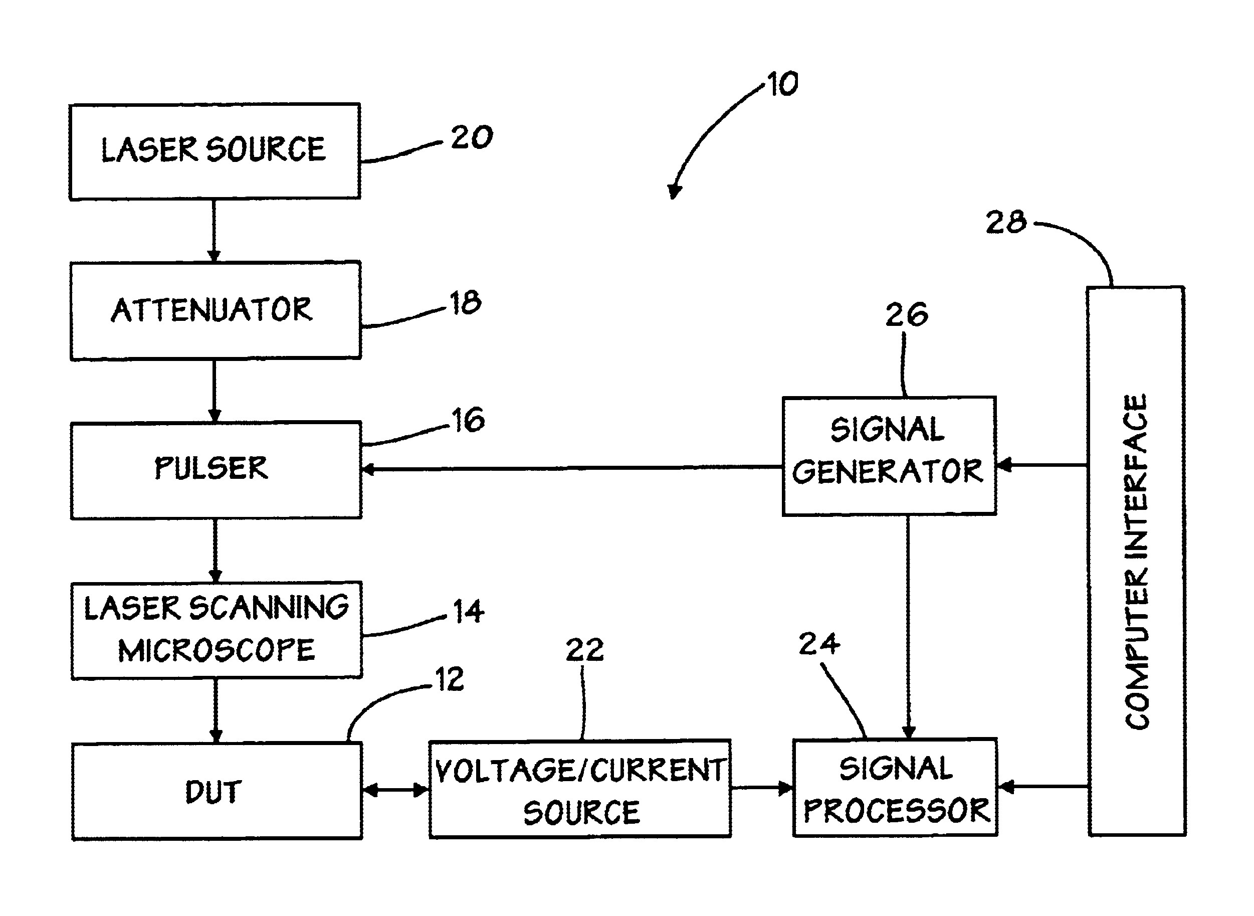
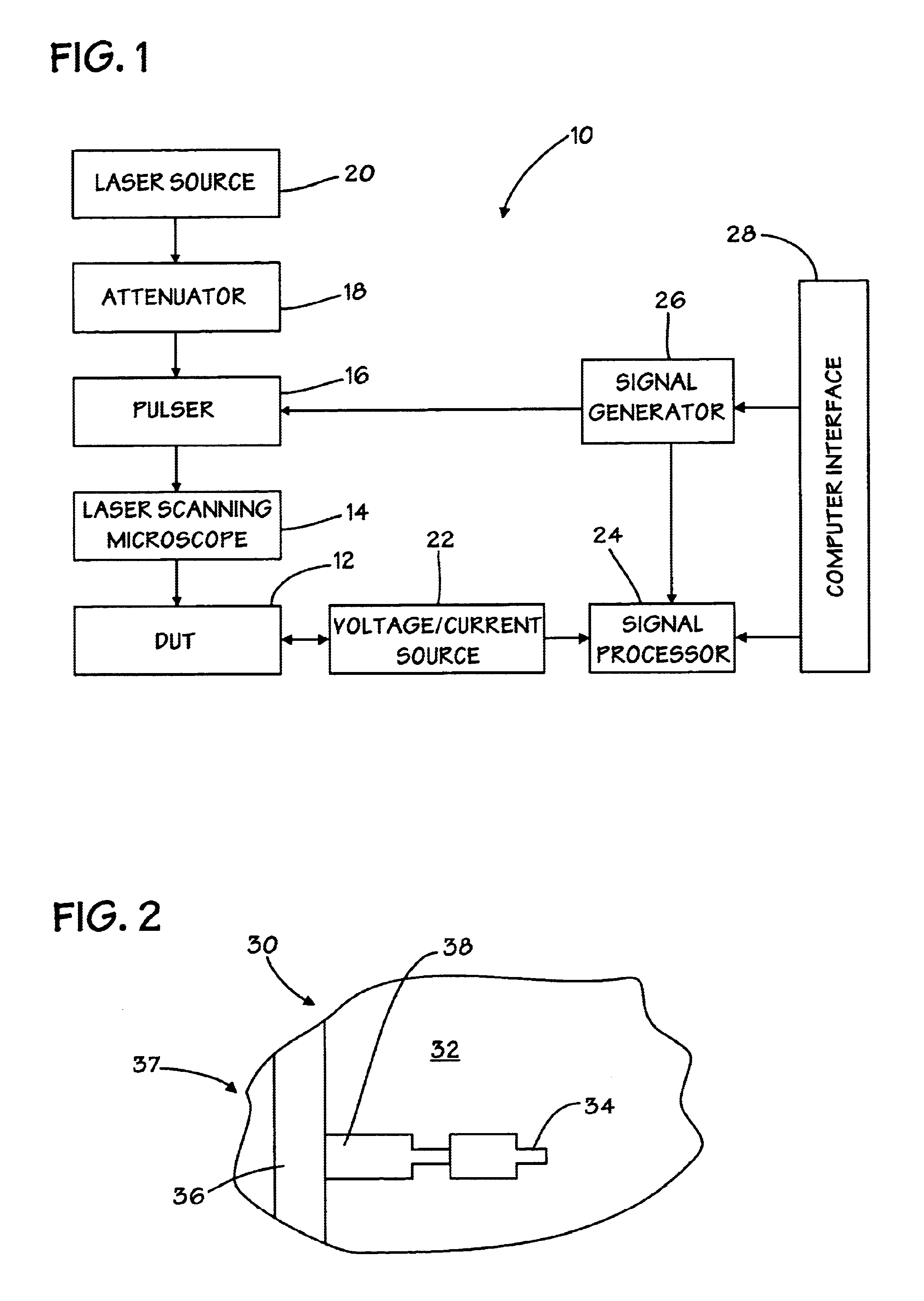
[0018]In the drawings described below, reference numerals are generally repeated where identical elements appear in more than one figure. Turning now to the drawings, and in particular to FIG. 1, therein is shown a block diagram of an exemplary embodiment of an inspection system 10 in accordance with the present invention. The inspection system 10 is designed to image a device under test (“DUT”) 12 by means of laser induced techniques. The DUT 12 may be any of a myriad of integrated circuit devices, such as, for example, diodes, transistors, capacitors, local interconnects, or the like. The system 10 includes a laser scanning microscope (“LSM”) 14, a pulser 16, an attenuator 18 and a laser source 20. A voltage / current source and detection circuit 22 (“detection circuit 22”) is provided to bias the DUT 12. A signal processor 24 is provided to acquire signals from the voltage / current source 22. A signal generator 26 may be provided to synchronize the pulser 16 with the voltage / current...


PUM


Abstract

Apparatus for and methods of inspection using laser beam induced alteration are provided. In one aspect, an apparatus is provided that includes a laser scanning microscope for directing a laser beam at a circuit structure and a source for biasing and thereby establishing a power condition in the circuit structure. A detection circuit is provided for detecting a change in the power condition in response to illumination of the circuit structure by the laser beam and generating a first output signal based on the detected change. A signal processor is provided for processing the first output signal and generating a second output signal based thereon. A control system is operable to scan the laser beam according to a pattern that has a plurality of pixel locations, whereby the laser beam may be moved to a given pixel location and allowed to dwell there for a selected time before being moved to another pixel location.

Description

BACKGROUND OF THE INVENTION[0001]1. Field of the Invention[0002]This invention relates generally to semiconductor processing, and more particularly to apparatus for laser beam induced phenomena inspection of integrated circuits and to methods of using the same.[0003]2. Description of the Related Art[0004]Fault-isolation techniques are critical to the development and manufacture of large-scale integrated circuits such as microprocessors. Examples of such techniques include those methodologies which exploit thermal beam induced phenomena such as Thermally Induced Voltage Alteration (“TIVA”), Seebeck Effect Imaging (“SEI”) and Infrared Laser Optical Beam Induced Resistance Change (“IR-OBIRCH”). These techniques are often effective in localizing electrical opens and shorts that can be significant manufacturing concerns.[0005]TIVA and SEI utilize a scanning infrared laser to isolate a defect within a die by thermally altering the defect's electrical characteristics. The basic setup uses ...

Claims


Application Information

Patent Timeline
IPC IPC(8): G01R31/28G01R31/305G01R31/311
CPCG01R31/311
Inventor BRUCE, MICHAELDABNEY, GREGORY A.MUTHUPALANIAPPAN, PALANIAPPANCHIN, JIANN MINWILCOX, RICHARD JACOBGILFEATHER, GLENDAVIS, BRENNANPHANG, JACOBCHUA, CHOON MENGKOH, LIAN SERNG, HOO-YINTAN, SOON HUAT
Owner GLOBALFOUNDRIES INC
Why Eureka
Try Eureka