

Laser scanning microscope, semiconductor laser light source unit, scanning unit for a laser scanning microscope, and method of connecting semiconductor light source to scanning microscope
a scanning microscope and laser scanning technology, applied in the direction of fluorescence/phosphorescence, luminescent dosimeters, optical radiation measurement, etc., can solve the problems that the loss of the beam or the remanence of the astigmatic difference cannot be avoided, and the light source and the lens system cannot be efficiently optically combined with each other
- Summary
- Abstract
- Description
- Claims
- Application Information
AI Technical Summary
Problems solved by technology
Method used
Image

Examples
first embodiment
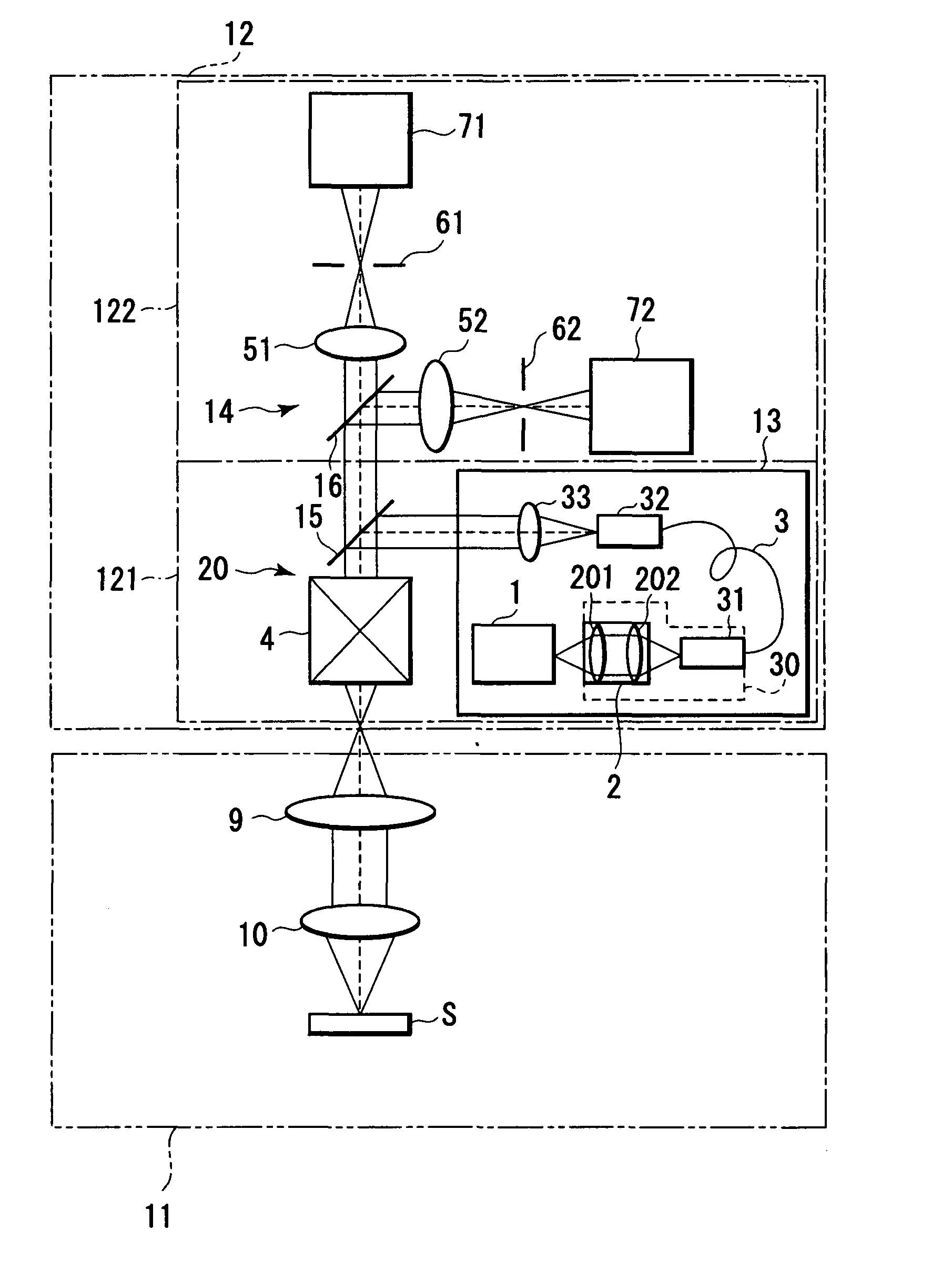
[0021]FIG. 1 is a view showing a structure of a two-channel detecting / laser scanning confocal microscope according to the present invention. The microscope shown in FIG. 1 comprises a microscope section 11 and a laser scanning / detecting system main body 12 (scanning optical system main body). The microscope section 11 and the laser scanning / detecting system main body 12 are configured by independent housings, respectively. When the laser scanning / detecting system main body 12 is attached to the microscope section 11, a laser scanning confocal microscope is configured.
[0022]The microscope section 11 includes an image forming lens 9 and an object lens 10 as a main optical system. The laser scanning / detecting system main body 12 has a scanning section 121 and a detection section 122. The scanning section 121 includes a light source section 13 and a scanning optical system 20 in one housing. The detection section 122 includes therein a detection optical system 14. It is to be noted that...
second embodiment
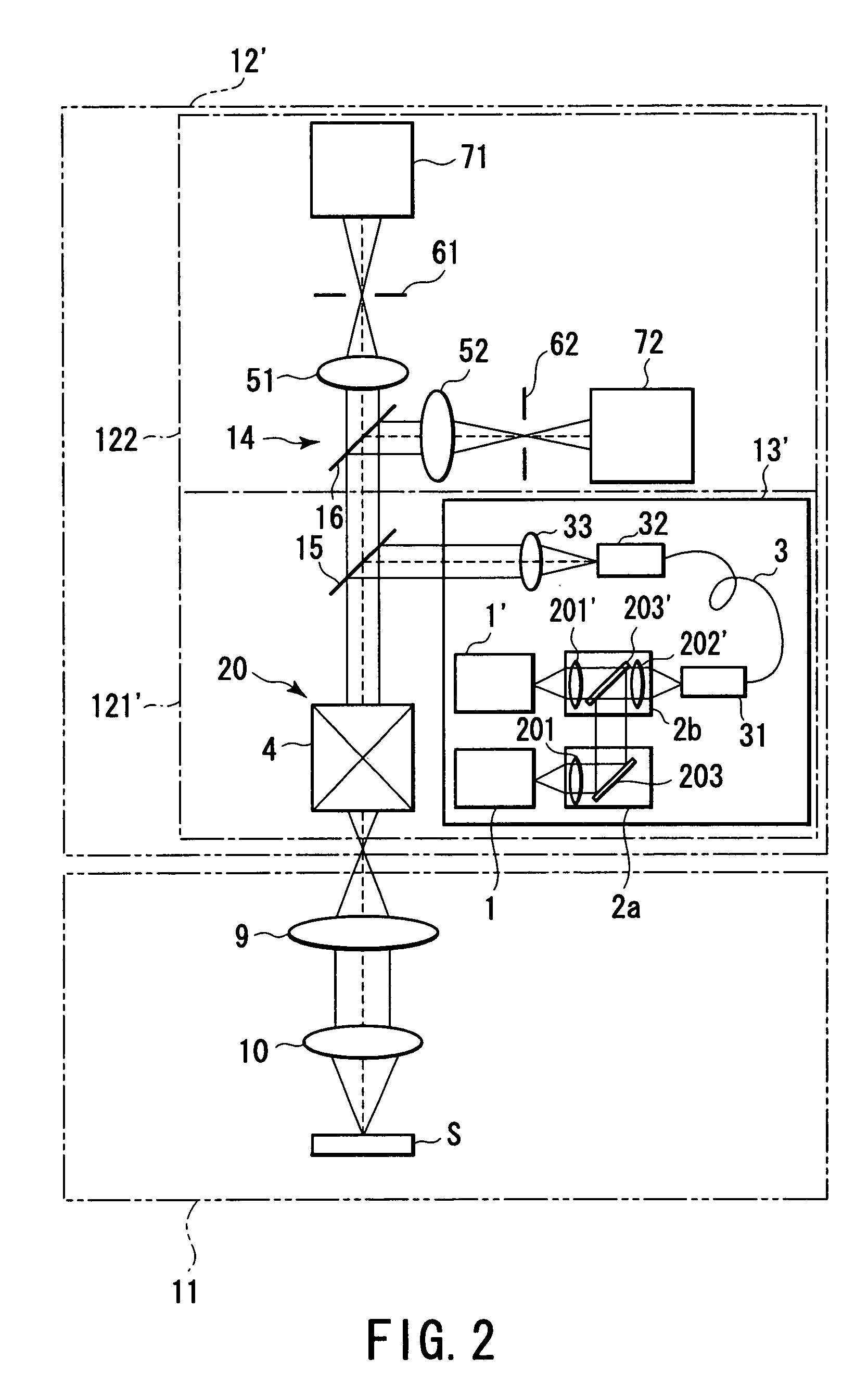
[0030]FIG. 2 is a view showing a structure of a two-channel detecting / laser scanning confocal microscope according to the present invention. In FIG. 2, like reference numerals denote parts equal to those in FIG. 1.
[0031]In an apparatus structure of FIG. 2, as parts different from the first embodiment, two types of semiconductor lasers 1 and 1′ (semiconductor laser diodes: light sources manufactured by a semiconductor process) having different wavelengths are used as light sources of a light source section 13′ in a scanning section 121′ configuring a laser scanning / detecting system main body 12′, and two beam shaping sections 2a and 2b are provided. The beam shaping section 2a has a spherical lens 201 and a deflection mirror 203. The beam shaping section 2b has a set of spherical lenses 201′ and 202′ and an optical member 203′.
[0032]If the semiconductor lasers 1 and 1′ have different wavelengths, a dichroic mirror is used as an optical member203′. This dichroic mirror has a character...
third embodiment
[0036]FIG. 3 is a view showing a structure of a two-channel detecting / laser scanning confocal microscope according to the present invention. In FIG. 3, like reference numerals denote parts equal to those in FIGS. 1 and 2.
[0037]In an apparatus structure illustrated in FIG. 3, as parts different from the first and second embodiments, two types of semiconductor lasers 1 and 1′ (semiconductor laser diodes: light sources manufactured by a semiconductor process) having different wavelengths are used as light sources of a light source section 13″ in a scanning section 121″ configuring a laser scanning / detecting system main body 12″, and two beam shaping sections 2 and 2′ and two types of optical fibers 3 and 3′ are provided. Further, the light source section 13″ comprises fiber incident optical systems 31 and 31′, fiber radiation optical systems 32 and 32′, lenses 33 and 33′ and an optical member 34. The beam shaping section 2′ has a set of spherical lenses 201′ and 202.
[0038]When the semi...
PUM
 Abstract
Description
Claims
Application Information