A kind of mosfet that improves UIS avalanche tolerance and preparation method thereof

An avalanche tolerance and consistent technology, applied in semiconductor/solid-state device manufacturing, semiconductor devices, electrical components, etc., can solve the problem of low avalanche breakdown tolerance, achieve the effect of improving avalanche tolerance and robustness, and improving breakdown voltage

Active Publication Date: 2021-03-16
ANHUI UNIVERSITY OF TECHNOLOGY
View PDF5 Cites 0 Cited by
  • Summary
  • Abstract
  • Description
  • Claims
  • Application Information

AI Technical Summary

Problems solved by technology

[0007] Aiming at the problem of low avalanche breakdown tolerance of MOSFET in the prior art, the present invention provides a MOSFET with improved UIS avalanche tolerance and a preparation method thereof

Method used


Image

  • A kind of mosfet that improves UIS avalanche tolerance and preparation method thereof
  • A kind of mosfet that improves UIS avalanche tolerance and preparation method thereof
  • A kind of mosfet that improves UIS avalanche tolerance and preparation method thereof

Examples


Embodiment 1

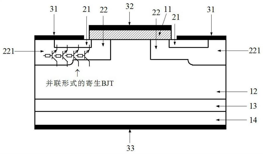
[0042] combine figure 2 , 3 , a MOSFET for improving UIS avalanche tolerance in this embodiment includes a second conductivity type doped source region 21, a first conductivity type doped base region 22 and a semi-insulating region 222, and a second conductivity type doped source region 22. The region 21 is located on top of the semi-insulating region 222 , and the base region 22 doped with the first conductivity type is located on the side of the source region 21 and the semi-insulating region 222 doped with the second conductivity type.

[0043] The existence of the semi-insulating region 222 reduces the area where parasitic BJTs exist, that is, reduces the number of parasitic BJTs, but there are still a small amount of parasitic BJTs under the channel region, but due to the great reduction in the number of parasitic BJTs, the Under UIS conditions, the current in the MOSFET limits the temperature increase, and the avalanche breakdown time of the MOSFET is increased from th...

Embodiment 2

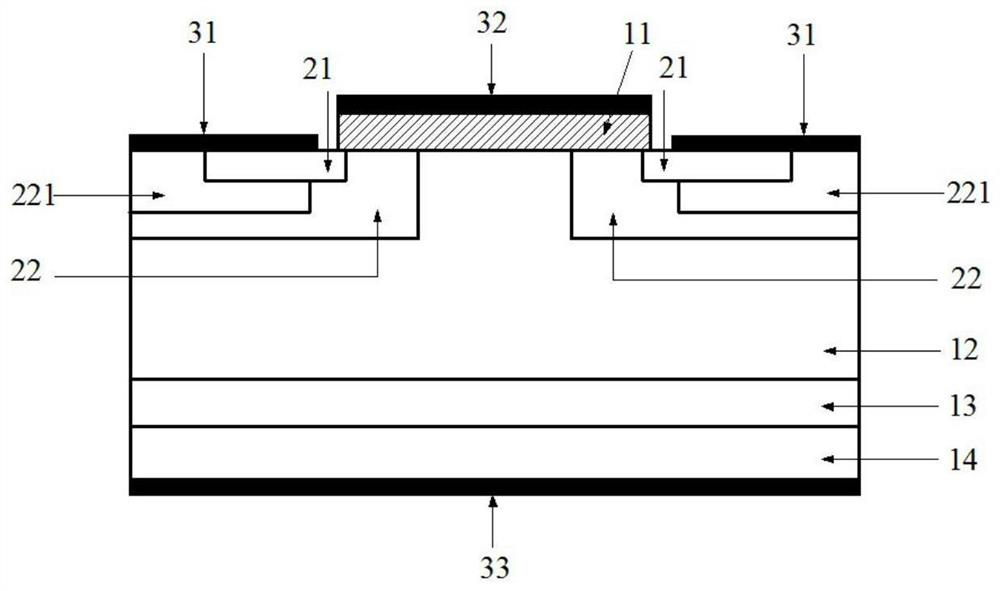
[0048] combine figure 2 , 3 , a MOSFET with improved UIS avalanche tolerance in this embodiment is further improved on the basis of Embodiment 1. The depth of the base region 22 doped with the first conductivity type is the same as the depth of the source region 21 and the semi-insulating region doped with the second conductivity type. The sum of the heights of the regions 222 is equal. The width ratio of the base region 22 doped with the first conductivity type and the source region 21 doped with the second conductivity type is 1:1-3. For specific applications, you can choose values ​​such as 1:1; 1:2; 1:3; 1:1.5; 1:2.8.

[0049] Precisely control the effective width of the conductive channel formed by the base region 22 doped with the first conductivity type, and does not change due to the introduction of the semi-insulating region 222 to ensure the threshold voltage, on-resistance, transconductance, output characteristics, etc. of the MOSFET The parameters do not change...

Embodiment 3

[0051] combine figure 2 , 3 , a MOSFET with improved UIS avalanche tolerance in this embodiment is further improved on the basis of Embodiments 1 and 2. The width of the source region 21 doped with the second conductivity type is the same as the width of the semi-insulating region 222 .

[0052] It is ensured that the effective channel length of the MOSFET does not change due to the introduction of the semi-insulating region 222, and that parameters such as threshold voltage, on-resistance, transconductance, and output characteristics of the MOSFET do not change due to the introduction of the semi-insulating region.


PUM


Abstract

The invention discloses a MOSFET for improving UIS avalanche tolerance and a preparation method thereof, belonging to the technical field of high-voltage power electronics. It includes a source region doped with the second conductivity type, a base region doped with the first conductivity type and a semi-insulating region, the source region doped with the second conductivity type is located on top of the semi-insulated region, and the base region doped with the first conductivity type is located at the The source region and one side of the semi-insulating region doped with the second conductivity type. The semi-insulating region is firstly implanted with impurities of the second conductivity type to achieve anti-doping to form an electrically neutral layer, and then relies on ion implantation of amphoteric impurity elements to form a semi-insulating region. On the basis of not affecting the key parameters such as MOSFET threshold voltage and on-state resistance, by reducing the area where the MOSFET parasitic transistor exists, it can greatly improve the avalanche tolerance of MOSFET for the problem of low avalanche breakdown tolerance of MOSFET in the prior art , robustness, ability to withstand high current, breakdown voltage and reliability.

Description

technical field [0001] The invention relates to the technical field of high-voltage power electronics, in particular to a MOSFET for improving UIS avalanche resistance and a preparation method thereof. Background technique [0002] With the continuous improvement of performance requirements of power conversion devices, higher requirements are put forward for power MOS transistor devices that undertake power conversion functions, one of which is to have high avalanche resistance in the unclamped inductive load switching process (UIS). , that is, it has a high resistance to UIS avalanche breakdown. This is because the energy stored in the inductive load under UIS conditions needs to be fully released by the power MOS transistor when it is turned off. At this time, the high current stress in the circuit is very high. It is easy to cause device failure, so the level of avalanche breakdown tolerance is one of the important indicators to reflect the performance of power MOS transi...

Claims


Application Information

Patent Timeline
Patent Type & Authority Patents(China)
IPC IPC(8): H01L29/06H01L29/78H01L21/336
CPCH01L29/0611H01L29/66477H01L29/78H01L29/7802H01L29/0653H01L29/66068H01L29/1608H01L29/167
Inventor 王兵周郁明
Owner ANHUI UNIVERSITY OF TECHNOLOGY
Why Eureka
Try Eureka