Mask and manufacturing method thereof

A manufacturing method and mask technology, applied in semiconductor/solid-state device manufacturing, ion implantation plating, coating, etc., can solve the problems affecting the deposition quality of organic light-emitting layers, and the quality and accuracy of metal masks cannot be well satisfied Requirements, issues affecting product quality, etc., to achieve the effect of improving restrictions, increasing robustness, and improving accuracy

Active Publication Date: 2018-10-12
NINGBO SEMICON INT CORP
View PDF5 Cites 5 Cited by
  • Summary
  • Abstract
  • Description
  • Claims
  • Application Information

AI Technical Summary

Problems solved by technology

The opening quality and opening position accuracy of the metal mask directly affect the deposition quality of the organic light-emitting layer, which in turn affects the quality of later products
At present, the metal mask processing technology of OLED is usually prepared by chemical etching using Invar alloy (INVAR, also known

Method used


Image

  • Mask and manufacturing method thereof
  • Mask and manufacturing method thereof
  • Mask and manufacturing method thereof

Examples


Example Embodiment

[0053] Example one

[0054] In view of the foregoing technical problems, the present invention proposes a mask, which mainly includes:

[0055] A substrate having a first surface and a second surface opposite to each other, the substrate has a plurality of openings penetrating the substrate, and the material of the substrate is a material capable of performing a semiconductor etching process;

[0056] A mask pattern layer located on the first surface, the material of the mask pattern layer is a material capable of performing a semiconductor etching process;

[0057] The mask pattern layer has a pattern area and a shielding area, each pattern area has at least one through hole, the opening exposes the pattern area, and each of the openings is opposite to and exposes the pattern area For all through holes in the pattern area, the shielding area is located outside the pattern area and opposite to the substrate.

[0058] The mask of the present invention is made by deposition, photolithogr...

Example Embodiment

[0083] Example two

[0084] The invention also provides a method for manufacturing a mask, such as Figure 7 As shown, it mainly includes the following steps:

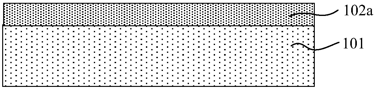
[0085] Step S1, providing a substrate having a first surface and a second surface opposite to each other, and a mask layer is formed on the first surface of the substrate;
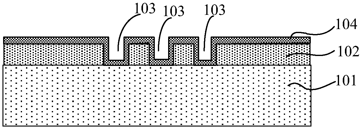
[0086] Step S2, according to a predetermined pattern, use a semiconductor etching process to etch the mask layer to form a mask pattern layer. The mask pattern layer has a pattern area and a shielding area, and each pattern area has at least one pass. Hole, the shielding area is located outside the graphic area;
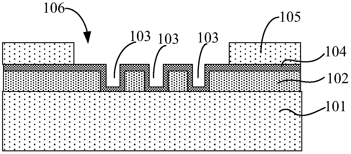
[0087] Step S3, etching the substrate from the second surface by a semiconductor etching process to form a plurality of openings penetrating the substrate, wherein the openings expose the pattern area.

[0088] Below, reference Figure 1A to Figure 1J The manufacturing method of the mask of the present invention will be described in detail, in whic...

Example Embodiment

[0137] Example three

[0138] It is worth mentioning that in order to obtain the mask in the first embodiment, the order of the method steps in this embodiment can also be exchanged to prepare and obtain the corresponding mask, for example, in order to obtain image 3 In the mask structure, you can also perform the following steps:


PUM

PropertyMeasurementUnit
Thicknessaaaaaaaaaa

Abstract

The invention provides a mask and a manufacturing method thereof. The mask comprises a substrate and a mask pattern layer positioned on the first surface; the substrate has a first surface and a second surface which are arranged oppositely; multiple openings for running through the substrate are formed in the substrate; the substrate material is a material which can be subjected to a semiconductoretching process; the mask pattern layer material is a material which can be subjected to a semiconductor etching process; the mask pattern layer has pattern regions and shielding regions; at least one through hole is formed in each pattern region; the openings expose the pattern regions; each opening is opposite to one pattern region and exposes all through holes in the corresponding pattern region; and the shielding regions are positioned outside the pattern regions and opposite to the substrate. The mask is high in quality and higher in precision; and when the mask is used for an evaporation process of an organic layer, the deposition quality of the organic layer can be improved, and quality of a post-period product is improved.

Description

technical field [0001] The invention relates to the technical field of semiconductors, in particular to a mask and a manufacturing method thereof. Background technique [0002] Compared with the current liquid crystal display technology, Organic Light-Emitting Dide (OLED) has the advantages of large viewing angle, bright colors, and low power consumption. In recent years, the speed of industrialization has advanced by leaps and bounds. [0003] In the current manufacturing process of the OLED display panel, the organic light-emitting layer is usually formed by evaporation, and the evaporation of the organic light-emitting layer generally uses a metal mask. The opening quality and opening position accuracy of the metal mask directly affect the deposition quality of the organic light-emitting layer, which in turn affects the quality of later products. At present, the metal mask processing technology of OLED is usually prepared by chemical etching using Invar alloy (INVAR, als...

Claims


Application Information

Patent Timeline
IPC IPC(8): H01L51/56C23C14/04
CPCC23C14/042H10K71/166
Inventor 刘孟彬罗海龙
Owner NINGBO SEMICON INT CORP
Why Eureka
Try Eureka