Device structure and implementation method for improving GaN L-FER reverse breakdown voltage

A technology of reverse breakdown voltage and device structure, which is applied in the field of microelectronics, can solve the problems of diode on-resistance affecting forward current characteristics, increasing the size of rectifier tubes, and decreasing response speed, so that the forward characteristics will not deteriorate, Improve the reverse breakdown voltage, easy to achieve the effect

Active Publication Date: 2018-10-16
PEKING UNIV
View PDF5 Cites 0 Cited by
  • Summary
  • Abstract
  • Description
  • Claims
  • Application Information

AI Technical Summary

Problems solved by technology

[0005] At present, the main methods to improve the reverse breakdown voltage of GaN L-FER are: 1. Increase the length of the anode gate to suppress the DIBL effect, but the channel below the anode gate of L-FER is normally off, and the extension of the normally off channel will inevitably increase The on-resistance of the diode affects its forward current characteristics; 2. Add a normally-on channel to the short-channel device. In the case of reverse bias, the normally-on channel can share the reverse voltage applied to the normally-off channel. Bias voltage, this method can suppress the reverse leakage and increase the breakdown voltage but increases the size of the rectifier tube, and the increase in capacitance leads to a decrease in response speed

Method used


Image

  • Device structure and implementation method for improving GaN L-FER reverse breakdown voltage
  • Device structure and implementation method for improving GaN L-FER reverse breakdown voltage
  • Device structure and implementation method for improving GaN L-FER reverse breakdown voltage

Examples


Embodiment Construction

[0032] In the following, the present invention will be described more fully with reference to the accompanying drawings, in which embodiments and their realization are shown, the described embodiment is only one form of realization in the present invention, that is, the present invention should not be interpreted are limited to the examples set forth herein. Based on the embodiment, the scope of the present invention is fully conveyed to those skilled in the art.

[0033] Hereinafter, exemplary embodiments of the present invention will be described in more detail with reference to the accompanying drawings.

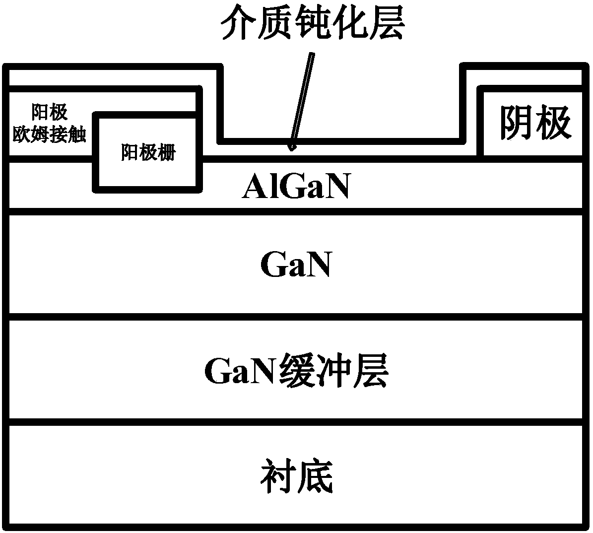
[0034] refer to figure 2 , the device structure includes a substrate, a GaN or AlN buffer layer, an intrinsic GaN channel layer, an intrinsic AlGaN barrier layer, an anode double Schottky layer, and a dielectric passivation layer in sequence from bottom to top. Its preparation method comprises the following specific steps:

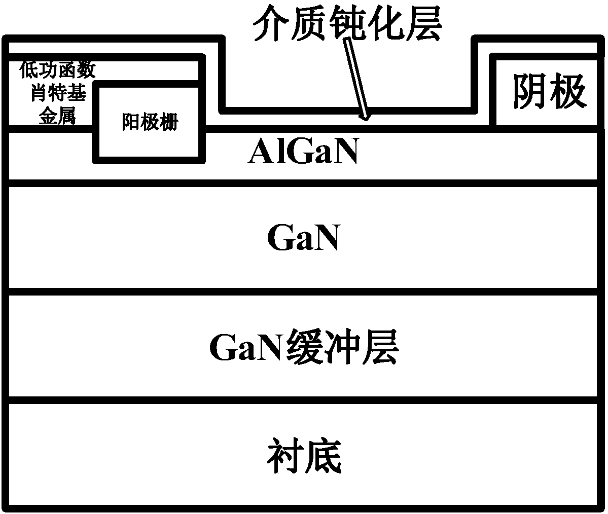
[0035] (1) if image 3 As shown, firstly, ...


PUM


Abstract

The invention discloses a device structure for improving a GaN L-FER reverse breakdown voltage and a fabrication method thereof. The structure includes a substrate, a GaN or AlN buffer layer, an intrinsic GaN channel layer, and an intrinsic AlGaN barrier layer, dielectric passivation layer, anode double Schottky contact, and cathode ohmic contact. The AlGaN/GaN heterojunction material is epitaxially grown on the substrate, and after the ohmic contact and planar isolation are formed on the structure, the anode structure of the double Schottky contact is further formed, and finally the passivation layer is deposited to achieve passivation of the device. The device structure utilizes the anode structure of the double Schottky contact, and the Schottky contact plays a certain shielding effecton the high voltage in the reverse breakdown process, Thereby reducing the leakage current injected from the anode through the channel barrier layer or the buffer layer of the device to the cathode, further increasing the reverse breakdown voltage of the device. The implementation method is simple and can greatly improve the reverse breakdown voltage of GaN L-FER, thereby broadening its application in the field of power electronics.

Description

technical field [0001] The invention belongs to the technical field of microelectronics and relates to the manufacture of GaN power electronic devices Background technique [0002] In recent years, gallium nitride materials have attracted widespread attention due to their good properties such as large band gap, strong breakdown electric field, high thermal conductivity, and high saturation velocity. The extremely high-concentration two-dimensional electron gas formed by the strong polarization effect of AlGaN / GaN heterojunction in gallium nitride materials plays an important role in the field of high-speed, high-power and withstand voltage electronic devices. [0003] Rectification characteristics play an important role in electronic systems. As a multi-sub-device, GaN lateral field effect rectifier (L-FER) has a fast response speed and has broad application prospects. However, despite its good material properties and heterojunction properties, the reverse breakdown voltage...

Claims


Application Information

Patent Timeline
Patent Type & Authority Applications(China)
IPC IPC(8): H01L29/06H01L29/45H01L29/47H01L21/335H01L29/778
CPCH01L29/0603H01L29/452H01L29/475H01L29/66462H01L29/778
Inventor 王茂俊高静楠尹瑞苑郝一龙
Owner PEKING UNIV
Why Eureka
Try Eureka