Ultra-wideband planar dual-beam slow wave structure

A slow-wave structure and ultra-broadband technology, which is applied to the circuit components of the time-of-flight electron tube, the shell/container of the time-of-flight electron tube, etc., can solve the problems of poor transmission characteristics and narrow bandwidth

Active Publication Date: 2018-10-19
UNIV OF ELECTRONICS SCI & TECH OF CHINA
View PDF5 Cites 4 Cited by
  • Summary
  • Abstract
  • Description
  • Claims
  • Application Information

AI Technical Summary

Problems solved by technology

[0004] The traditional planar slow wave structure includes microstrip slow wave structure and strip slow wave structure, in which the electric field energy of the microstrip slow wave structure is mainly concentrated in its dielectric substrate, and with the decrease of the thickness of the dielectric substrate and the increase of its dielectric constant It is more and more obvious that there are disadvantages such as poor transmission characteristics and narrow bandwidth; while the dispersion of the banded slow wave structure has a large correlation with many structural parameters, and the dispersion is usually strong under the limitations of the existing processing conditions.

Method used


Image

  • Ultra-wideband planar dual-beam slow wave structure
  • Ultra-wideband planar dual-beam slow wave structure
  • Ultra-wideband planar dual-beam slow wave structure

Examples


Embodiment

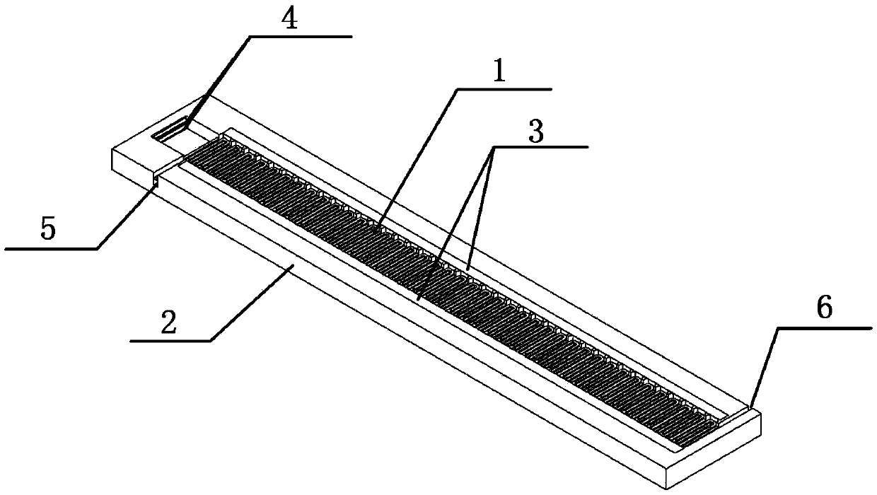
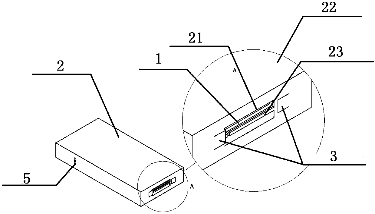
[0020] figure 1 It is a structural diagram of a specific embodiment of the ultra-broadband planar double-injection slow-wave structure of the present invention. In order to show the inner structure of the ultra-broadband planar double-injection slow-wave structure more clearly, figure 1 Part of the metal casing is hidden in it. Such as figure 1 As shown, the ultra-broadband planar double-injection slow wave structure of the present invention includes a planar metal slow wave line 1, a metal shell 2 and two dielectric support rods 3, which are the same as the conventional slow wave structure, and electrons from the electron gun will be added at appropriate positions as required. Incident port 4, signal input port 5 and signal output port 6.

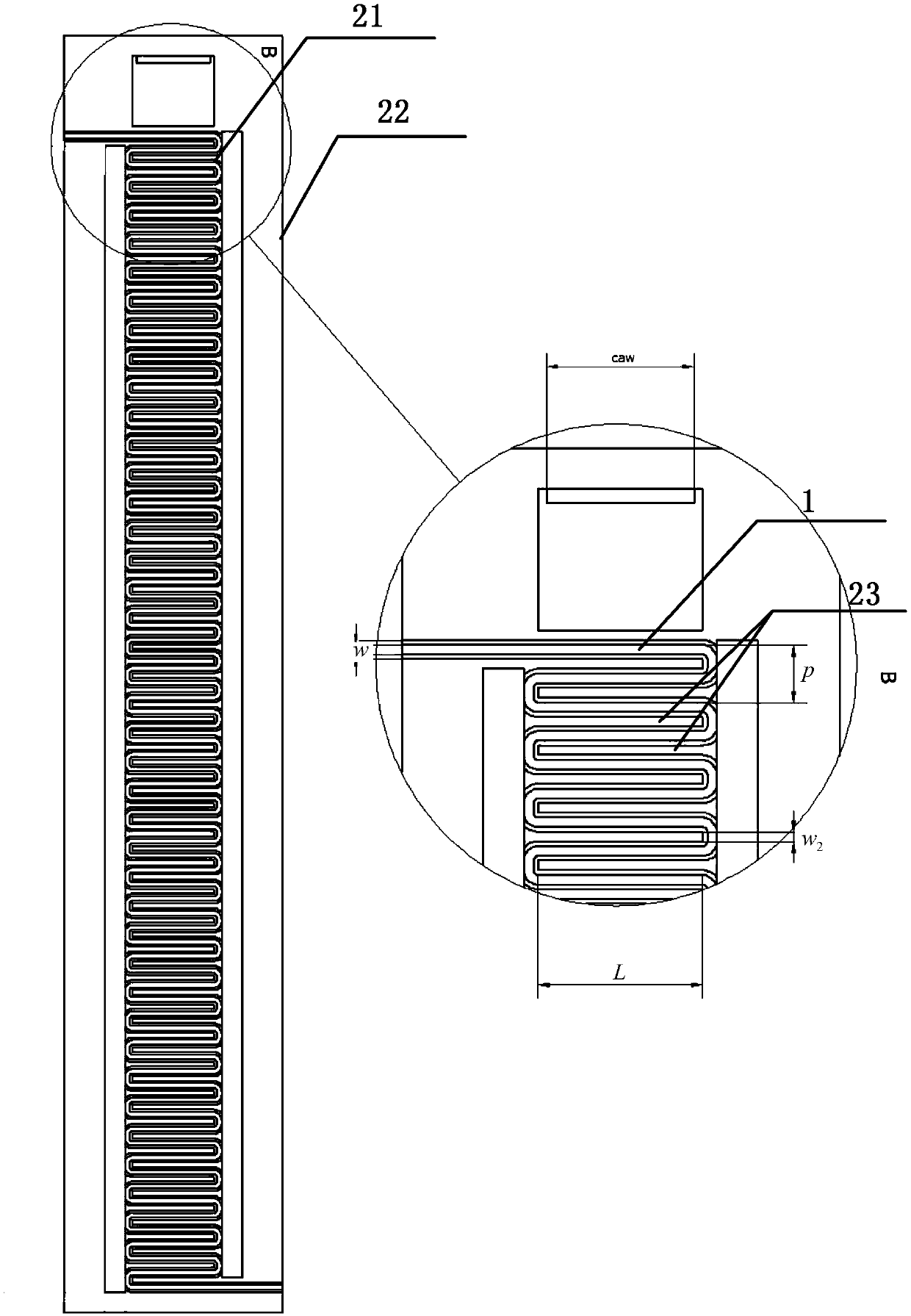
[0021] figure 2 yes figure 1 A top-down cross-sectional view of the ultra-broadband planar double-injection slow-wave structure shown. figure 2 The section in is parallel to the plane where the planar metal slow-wave line 1 is loca...


PUM


Abstract

The invention discloses an ultra-wideband planar dual-beam slow wave structure. The ultra-wideband planar dual-beam slow wave structure comprises a planar metal slow wave wire, a metal shell and two dielectric support rods; the planar metal slow wave wire comprises straight metal lines and curved metal lines alternatively connecting the straight metal lines; extension sections are disposed on twoopposite side surfaces of the inner layer of the metal shell, and an opening is disposed between every two adjacent extension sections; the two dielectric support rods are fixed between the inner andouter layers on both sides of the metal shell; parts of the side surfaces of the dielectric support rods are exposed from the openings between the extension sections, are in surface contact with the curved metal lines of the planar metal slow wave wire, and clamp the planar metal slow wave wire to make the planar metal slow wave wire suspend within the inner cavity of the metal shell; each of theextension sections of each side surface of the inner layer extends into the corresponding opening facing the side surface, of the planar metal slow wave wire. The invention can reduce the dispersion characteristics and improve the coupling impedance under the premise of ensuring a large bandwidth.

Description

technical field [0001] The invention belongs to the technical field of ribbon beam traveling wave tube slow-wave systems, and more specifically relates to an ultra-broadband planar double-injection slow-wave structure. Background technique [0002] As a microwave power device, traveling wave tubes have a very wide range of applications. For different application methods, traveling wave tubes have different characteristics. Generally speaking, the advantages of traveling wave tubes are bandwidth, high power, high gain, high efficiency, large gain and long life, etc., but in most cases, a traveling wave tube cannot have all the advantages at the same time. Rather, each has its own strengths, and traveling wave tubes with different advantages are applied to different fields. [0003] The slow-wave structure is a device for strengthening the interaction between moving electrons and electromagnetic fields in traveling-wave electronic devices, so that the energy of electron flow ...

Claims


Application Information

Patent Timeline
Patent Type & Authority Applications(China)
IPC IPC(8): H01J23/24H01J23/12
CPCH01J23/12H01J23/24
Inventor 许多师凝洁王禾欣何腾龙李新义王战亮宫玉彬
Owner UNIV OF ELECTRONICS SCI & TECH OF CHINA
Why Eureka
Try Eureka