Copper embedded block heat radiation substrate and manufacturing method therefor

A technology of heat-dissipating substrates and buried copper blocks, applied in circuit thermal devices, printed circuit components, etc., can solve the problems of large height deviation of copper bosses, low production efficiency, unstable quality, etc., to improve dimensional accuracy and solve easy problems. The effect of offset, improving processing efficiency and quality stability

Active Publication Date: 2018-10-19
KINWONG ELECTRONICS TECH LONGCHUAN
View PDF5 Cites 5 Cited by
  • Summary
  • Abstract
  • Description
  • Claims
  • Application Information

AI Technical Summary

Problems solved by technology

Chinese patent document CN104797085B discloses a method for manufacturing blind slots buried in copper blocks of circuit boards. It uses exposed photosensitive resist film to protect the circuit board parts that do not need to open blind slots, and uses etching to make blind slots. Due to the etching process The uniformity is good, and the wall of the blind groove is flat, which solves the problem that the bottom of the blind groove is easily produced by the traditional CNC machine tool.
However, the above solutions all use single-sided heat dissipation, and the overall heat dissipation is still not good.
In addition, the buried copper block or copper boss in the prior art is made by CNC milling machine or laser cutting, which has the problems of large deviation in the height of the copper boss and unstable quality, which easily affects the heat dissipation effect of electronic components. The method with buried copper block has low production efficiency

Method used


Image

  • Copper embedded block heat radiation substrate and manufacturing method therefor
  • Copper embedded block heat radiation substrate and manufacturing method therefor
  • Copper embedded block heat radiation substrate and manufacturing method therefor

Examples


Embodiment 1

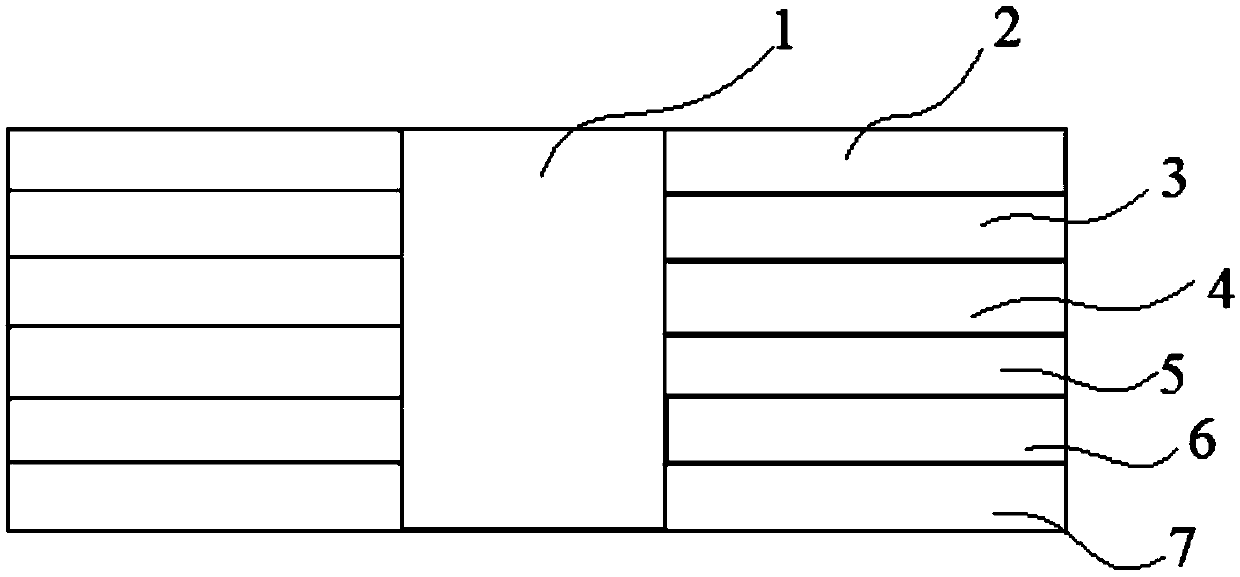
[0035] This embodiment provides a buried copper heat dissipation substrate, such as figure 1 As shown, the heat dissipation substrate includes a substrate body, and the substrate body is provided with a buried copper block through groove, and a heat dissipation copper block 1 is arranged in the buried copper block through groove, and the heat dissipation copper block 1 is a rectangular parallelepiped copper block. Its top surface and bottom surface are respectively flush with the top surface and bottom surface of the heat dissipation substrate, so that the top surface and bottom surface of the heat dissipation copper block 1 are exposed to the environment, and the heat dissipation effect is better.

[0036] Specifically, from top to bottom, the substrate body is composed of a top layer of copper foil 2, a top layer of optical core board 3, and a prepreg layer (the prepreg layer is two layers, and the first prepreg 4 is respectively from top to bottom) , the second prepreg 5), ...

Embodiment 2

[0039] This embodiment provides a buried copper heat dissipation substrate, such as figure 1As shown, the heat dissipation substrate includes a substrate body, and the substrate body is provided with a buried copper block through groove, and a heat dissipation copper block 1 is arranged in the buried copper block through groove, and the heat dissipation copper block 1 is a rectangular parallelepiped copper block. Its top surface and bottom surface are respectively flush with the top surface and bottom surface of the heat dissipation substrate, so that the top surface and bottom surface of the heat dissipation copper block 1 are exposed to the environment, and the heat dissipation effect is better.

[0040] Specifically, from top to bottom, the substrate body is composed of a top layer of copper foil 2, a top layer of optical core board 3, and a prepreg layer (the prepreg layer is two layers, and the first prepreg 4 is respectively from top to bottom) , the second prepreg 5), t...

Embodiment 3

[0043] This embodiment provides a buried copper heat dissipation substrate, such as figure 1 As shown, the heat dissipation substrate includes a substrate body, and the substrate body is provided with a buried copper block through groove, and a heat dissipation copper block 1 is arranged in the buried copper block through groove, and the heat dissipation copper block 1 is a rectangular parallelepiped copper block. Its top surface and bottom surface are respectively flush with the top surface and bottom surface of the heat dissipation substrate, so that the top surface and bottom surface of the heat dissipation copper block 1 are exposed to the environment, and the heat dissipation effect is better.

[0044] Specifically, from top to bottom, the substrate body is composed of a top layer of copper foil 2, a top layer of optical core board 3, and a prepreg layer (the prepreg layer is two layers, and the first prepreg 4 is respectively from top to bottom) , the second prepreg 5), ...


PUM

PropertyMeasurementUnit
thicknessaaaaaaaaaa
thicknessaaaaaaaaaa
lengthaaaaaaaaaa

Abstract

The invention discloses a copper embedded block heat radiation substrate comprising a substrate body, wherein the substrate body is provided with a copper embedded block via groove, a heat radiation copper block is arranged in the copper embedded block via groove, and a surface of the heat radiation copper block is level with a surface of the heat radiation substrate. The heat radiation copper block is arranged in the substrate, a top face and a bottom face of the heat radiation copper block are exposed from an outer part of the substrate, and the heat radiation substrate is enabled to have adouble face heat radiation structure; compared with a conventional copper embedded block PCB board only capable of single surface heat radiation, the copper embedded block heat radiation substrate disclosed in the invention is advantaged by improved heat radiation efficiency. The invention also discloses a manufacturing method for the copper embedded block heat radiation substrate; a two time etching method is adopted for manufacturing the heat radiation copper block of which double surfaces are exposed, size precision of the heat radiation copper block is improved in such a processing mannerthat a bottom part heat radiation copper block is manufactured after pressing operation, and copper blocks are bonded together via two time pressing operation; a problem that the copper blocks are prone to deviating, loosening, cracking and the like; copper block processing efficiency and quality stability can be improved.

Description

technical field [0001] The invention belongs to the technical field of printed circuit board production, and relates to a circuit board substrate and a manufacturing method thereof, in particular to a buried copper block heat dissipation substrate and a manufacturing method thereof. Background technique [0002] With the continuous development of electronic devices towards intelligence, miniaturization and portability, such as the popularity of dual cameras in smartphones and smart car lights, the power density of electronic devices is increasing. Part of it is used to do useful work, and most of it is converted into heat, which causes the internal temperature of the component to rise rapidly. If the heat is not dissipated in time, the continuous heating of electronic components will cause quality degradation, affect the stability of use and service life, and in severe cases It can also cause printed circuit board failure or even damage. [0003] Therefore, for electronic c...

Claims


Application Information

Patent Timeline
Patent Type & Authority Applications(China)
IPC IPC(8): H05K1/02
CPCH05K1/0203
Inventor 谭小林沙伟强张军
Owner KINWONG ELECTRONICS TECH LONGCHUAN
Why Eureka
Try Eureka