Super-thick copper PCB with inner and outer layers of 6OZ, and manufacturing method thereof

A PCB board, inner and outer layer technology, applied in the inner and outer layer 6OZ ultra-thick copper PCB board and its production field, can solve the problems of board thickness exceeding 2.5mm, poor thickness uniformity, cracking board, etc., and achieve the effect of ensuring thickness uniformity

Pending Publication Date: 2018-10-30
江门荣信电路板有限公司
View PDF0 Cites 13 Cited by
  • Summary
  • Abstract
  • Description
  • Claims
  • Application Information

AI Technical Summary

Problems solved by technology

Therefore, in the production process, the number of layers of ultra-thick copper PCB boards is increasing, but the problems caused by this are also highlighted, such as board thickness exceeding 2.5mm, poor thickness uniformity, or lack of glue, board explosion other risks

Method used


Image

  • Super-thick copper PCB with inner and outer layers of 6OZ, and manufacturing method thereof
  • Super-thick copper PCB with inner and outer layers of 6OZ, and manufacturing method thereof

Examples


Embodiment Construction

[0035] The present invention will be described in further detail below in conjunction with the embodiments in the accompanying drawings, but this does not constitute any limitation to the present invention.

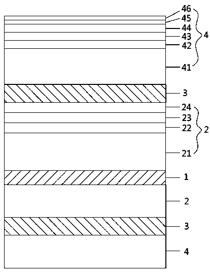
[0036] Such as figure 1 As shown, a kind of inner and outer layer 6OZ ultra-thick copper PCB board provided by the present invention is composed of a core board 1, an inner layer copper 2 electroplated on the upper and lower surfaces of the core board 1, a PP sheet 3 pressed on the inner layer copper 2 and The outer layer copper 4 is electroplated on the PP sheet 3; the total thickness of the finished PCB board is 1.4-1.6mm, wherein the thickness of the core board 1 is 0.1mm, and the minimum copper thickness of the inner layer copper 2 and the outer layer copper 4 is 6OZ (equivalent to 210μm), the thickness of the substrate excluding the outer layer copper 4 is 1.05-1.10mm.

[0037] The inner layer of copper 2 is composed of a layer of original base copper layer 21 cover...


PUM

PropertyMeasurementUnit
thicknessaaaaaaaaaa
thicknessaaaaaaaaaa
thicknessaaaaaaaaaa

Abstract

The invention discloses a super-thick copper PCB with inner and outer layers of 6OZ, and a manufacturing method thereof. The PCB is composed of a core board, inner-layer copper plated on the upper andlower surfaces of the core board, a PP sheet pressed on the inner-layer copper, and outer-layer copper plated on the PP sheet. The manufacturing method comprises the steps of cutting, removing smear,plating the full board, drying the film on the inner layer, etching the inner layer, AOI detection, browning, cutting and filling the PP sheet, laminating, milling the edge of the board, plating thefull board for the second time, drilling a hole, removing drill smear, drying the film on the outer layer, plating a pattern, etching the outer layer, secondary AOI detection, coating solder, millingthe board and electrical logging. According to the super-thick copper PCB provided by the invention, the inner-layer copper, the PP sheet and the outer-layer copper are sequentially arranged on the upper and lower surfaces of the core board that is 0.1mm thick to form a laminated structure, so that the overall thickness of the board is controlled to be 1.4-1.6mm, and the thickness uniformity of the PCB is ensured.

Description

technical field [0001] The invention relates to the technical field of printed circuit boards, more specifically, to a 6OZ ultra-thick copper PCB board with inner and outer layers and a manufacturing method thereof. Background technique [0002] Ultra-thick copper circuit board refers to a circuit board with an inner conductive circuit layer thickness greater than or equal to 100 μm. The ultra-thick copper circuit board has the advantages of being able to pass large currents and good heat dissipation performance, and better meet the needs of high-end markets such as the automotive electronics industry. The demand for circuit boards has great potential for market development. Therefore, in the production process, the number of layers of ultra-thick copper PCB boards is increasing, but the problems caused by this are also highlighted, such as board thickness exceeding 2.5mm, poor thickness uniformity, or lack of glue, board explosion and other risks. Contents of the inventi...

Claims


Application Information

Patent Timeline
Patent Type & Authority Applications(China)
IPC IPC(8): H05K1/09H05K3/00
CPCH05K1/09H05K3/00H05K2201/0338H05K2201/098
Inventor 曾建华
Owner 江门荣信电路板有限公司
Why Eureka
Try Eureka