TFT array substrate and liquid crystal display panel

An array substrate and display area technology, applied in optics, instruments, electrical and digital data processing, etc., can solve the problems of inability to fan out the size of the trace area, such as compression, inability to overlap, etc., to achieve reduced area, small size, and narrow borders. Effect

Active Publication Date: 2018-11-02
WUHAN CHINA STAR OPTOELECTRONICS TECH CO LTD
View PDF3 Cites 26 Cited by
  • Summary
  • Abstract
  • Description
  • Claims
  • Application Information

AI Technical Summary

Problems solved by technology

make image 3 The number of masks required for the TFT array substrate shown is 10, which can reduce the number of masks. However, please refer to Figure 4 , image 3 The shown fan-out area of ​​the TFT array substrate includes a plurality of first fan-out lines 801 and second fan-out lines 802. The first fan-out lines 801 are located on the first metal layer, and the second fan-out lines 802 are located on the second metal layer. The first fan-out lines 801 are respectively electrically connected to a plurality of data lines and the plurality of second fan-out lines 802 are respectively electrically connected to a plurality of touch traces 872, or the plurality of second fan-out lines 802 are respectively electrically connected to a plurality of data lines And the plurality of first fan-out lines 801 are respectively electrically connected to the plurality of touch-control lines 882, no matter which way, the fan-out lines connecting the multiple data lines are all located on the same metal layer, and cannot overlap with each other, so that the fan-out lines cannot be connected to each other. The size of the outgoing wiring area is compressed, and the larger the pixel density (PPI), the more obvious the problem that the size of the fan-out wiring area cannot be compressed, which limits the development of display panels in the direction of narrow borders

Method used


Image

  • TFT array substrate and liquid crystal display panel
  • TFT array substrate and liquid crystal display panel
  • TFT array substrate and liquid crystal display panel

Examples


Embodiment Construction

[0060] In order to further illustrate the technical means adopted by the present invention and its effects, the following describes in detail in conjunction with preferred embodiments of the present invention and accompanying drawings.

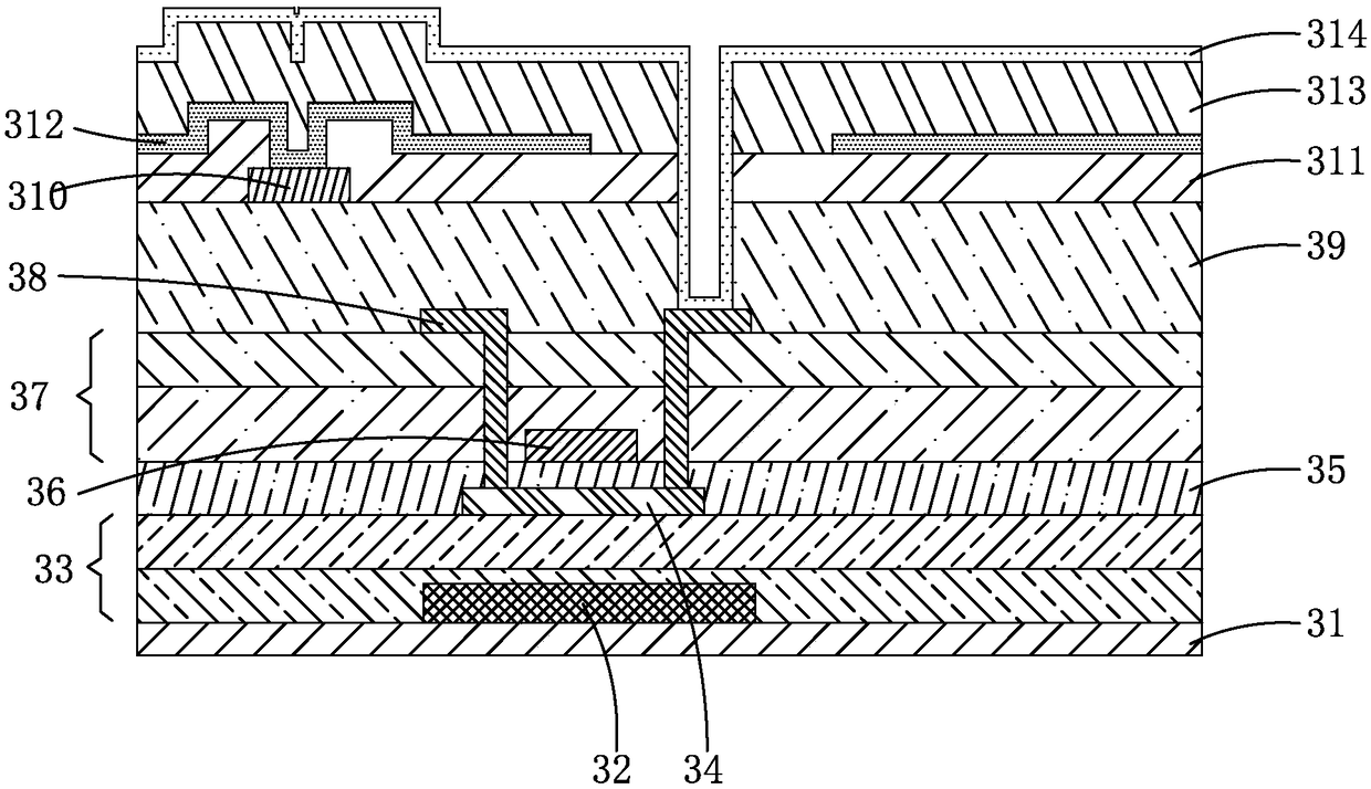
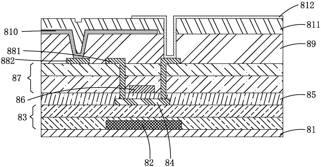
[0061] see Figure 5 and Figure 6 , The first embodiment of the TFT array substrate of the present invention includes a substrate 100, a first metal layer 200 disposed above the substrate 100, a first interlayer insulating layer 300 covering the first metal layer 200, and a first interlayer insulating layer 300 disposed on the first layer The second metal layer 400 on the interlayer insulating layer 300 , the second interlayer insulating layer 500 covering the second metal layer 400 , and the third metal layer 600 disposed on the second interlayer insulating layer 500 .

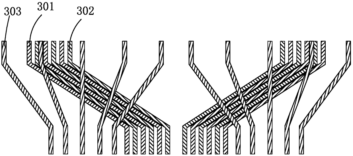
[0062] The substrate 100 includes an active display area 110 and a fan-out routing area 120 arranged in sequence. The first metal layer 200 includes a plurality of first f...


PUM


Abstract

The invention provides a TFT array substrate and a liquid crystal display panel. The TFT array substrate comprises a first metal layer, a first interlayer insulating layer, a second metal layer, a second interlayer insulating layer and a third metal layer which are sequentially arranged on a substrate and is characterized in that the first metal layer comprises a plurality of first fan-out wires located in a fan-out wiring area, the second metal layer comprises a plurality of second fan-out wires located in the fan-out wiring area, the third metal layer comprises a plurality of third fan-out wires located in the fan-out wiring area, two of the first fan-out wires, the second fan-out wires and the third fan-out wires are connected with a data line, and the other one of the first fan-out wires, and the second fan-out wires and the third fan-out wires is connected with a touch control wire. Due to the fact that the first interlayer insulating layer is arranged between the first fan-out wires and the second fan-out wires and the second interlayer insulating layer is arranged between the third fan-out wires and the second fan-out wires, the first fan-out wires, the second fan-out wiresand the third fan-out wires can be arranged in an overlapped manner, the area of the fan-out wiring area can be reduced effectively, and a narrow frame can be achieved.

Description

technical field [0001] The invention relates to the field of display technology, in particular to a TFT array substrate and a liquid crystal display panel. Background technique [0002] In the field of display technology, flat panel display devices such as Liquid Crystal Display (LCD) and Organic Light-Emitting Diode (OLED) displays have gradually replaced Cathode Ray Tube (CRT) display devices. The liquid crystal display device has many advantages such as a thin body, power saving, and no radiation, and has been widely used. [0003] Most of the liquid crystal display devices currently on the market are backlight liquid crystal display devices, which include a liquid crystal display panel and a backlight module. Generally, a liquid crystal display panel consists of a color filter (ColorFilter, CF) substrate, a thin film transistor (Thin Film Transistor, TFT) array substrate, a liquid crystal (Liquid Crystal, LC) and a sealant frame sandwiched between the color filter subst...

Claims


Application Information

Patent Timeline
Patent Type & Authority Applications(China)
IPC IPC(8): G02F1/1362G02F1/1368G02F1/1343G02F1/1333
CPCG02F1/13338G02F1/134309G02F1/13439G02F1/136227G02F1/136286G02F1/1368G02F1/1345G06F3/0412G06F3/04164G02F1/134363G02F1/136209G02F1/134318G02F1/13629G02F1/13685
Inventor 李亚锋邬金芳
Owner WUHAN CHINA STAR OPTOELECTRONICS TECH CO LTD
Why Eureka
Try Eureka