LED die bonding method

A technology of die-bonding and die-bonding machine, which is applied in electrical components, circuits, semiconductor devices, etc., can solve the problems of inability to achieve the quality of small-sized products, and achieve the effects of increasing production capacity, improving efficiency, and improving brightness

Inactive Publication Date: 2018-11-06
苏州市汇涌进光电有限公司
View PDF6 Cites 0 Cited by
  • Summary
  • Abstract
  • Description
  • Claims
  • Application Information

AI Technical Summary

Problems solved by technology

As the size of the product becomes smaller and smaller, the brackets and chips used are also getting smaller and smaller. In the process of LED packaging, the traditional die-bonding process can no longer meet the quality requirements of small-sized products.

Method used


Image

  • LED die bonding method
  • LED die bonding method

Examples


Embodiment 1

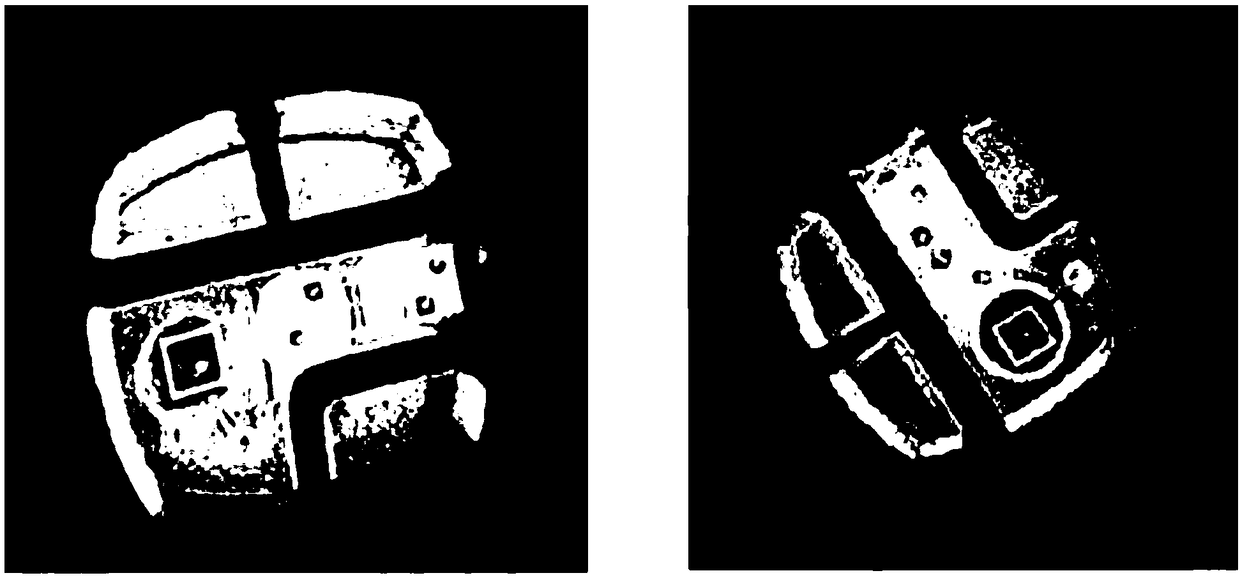
[0029] This embodiment provides a LED die-bonding method, including the following steps:

[0030] S1: Through the search and positioning function of the die bonder, after determining the position of the die bonded in the bracket cup, draw a bottom line at the die bond position;

[0031] S2: Fix the 350-800 mesh silk screen on the top of the working table of the glue brushing machine, fix and lock the screen through the wire frame and the screen locker, and then apply the primer to the screen; then apply the electrode layer of the chip Stick it on the blue film to expose the bottom layer of the chip, then place the obtained blue film chip on the working table of the glue brushing machine, so that the screen is 2mm higher than the chip; finally, the rubber scraper is driven by the manipulator to withstand the screen surface And press down until it touches the chip, scrape back and forth twice, then the manipulator drives the rubber scraper up, releases the screen lock, lifts the...


PUM


Abstract

The invention discloses an LED die bonding method. The method comprises the following steps of S1: determining a die bonding position on a bracket bowl cup through a die bonder; S2: coating a 350-800-mesh silk screen with primer, inverting a chip below the silk screen, and coating the back surface of the chip with the glue on the silk screen through a cementing machine; S3: adhering the back surface of the chip to the die bonding position, and meanwhile, applying a pressure; and S4: putting an obtained finished product into a baking oven for baking and curing. According to the LED die bondingmethod, the quality and the die bonding efficiency of LED products can be improved; and the method is suitable for die bonding of small-sized LED products.

Description

technical field [0001] The invention relates to the technical field of LED packaging, in particular to a method for bonding crystals of LED chips. Background technique [0002] Die bonding is also called Die Bond or die bonding. In the LED packaging industry, die bonding is the process of bonding the chip to the designated area of ​​the bracket through colloid to form a thermal path or electrical path, which provides conditions for the subsequent wiring connection. The traditional process is to use the crystal bonding equipment to take out the primer (epoxy) and place it in the bracket bowl. [0003] With the development of the LED packaging industry, the smaller and smaller product sizes have become the industry trend. At present, in the LED industry, the minimum product size has reached 0.8mm*0.8mm. As the product size becomes smaller and smaller, the brackets and chips used are also smaller and smaller. In the process of LED packaging, the traditional die-bonding process...

Claims


Application Information

Patent Timeline
Patent Type & Authority Applications(China)
IPC IPC(8): H01L33/62H01L33/64
Inventor 祝运芝
Owner 苏州市汇涌进光电有限公司
Why Eureka
Try Eureka