Waste PCB treatment device

A PCB board and processing device technology, which is applied in the field of waste PCB board recycling and processing devices, can solve the problems of automatic disassembly of PCB boards, automatic classification and recycling of electronic components, waste of resources, environmental hazards, etc.

Inactive Publication Date: 2018-11-13
HUZHOU HUINENG ELECTROMECHANICAL TECH CO LTD
View PDF0 Cites 0 Cited by
  • Summary
  • Abstract
  • Description
  • Claims
  • Application Information

AI Technical Summary

Problems solved by technology

[0003] The PCB board is a collection of glass fiber, resin, copper and tin. The metal content in the PCB board is about 40%. For the ever-increasing waste PCB boards and a large number of scraps from PCB board manufacturers, if there is no effective treatment method, it will be Harmful to the environment and a waste of resources
In the prior art, before the PCB board is crushed and sorted, the PCB board is not automatically disassembled and the electronic components are not automatically sorted and recycled

Method used


Image

  • Waste PCB treatment device
  • Waste PCB treatment device
  • Waste PCB treatment device

Examples


Embodiment Construction

[0023] In order to make the object, technical solution and advantages of the present invention clearer, the present invention will be further described in detail below in conjunction with the accompanying drawings and embodiments. It should be understood that the specific embodiments described here are only used to explain the present invention, not to limit the present invention.

[0024] It should be noted that the orientation terms such as up, down, left, and right in this embodiment are only relative concepts or refer to the normal use state of the product, and should not be regarded as limiting.

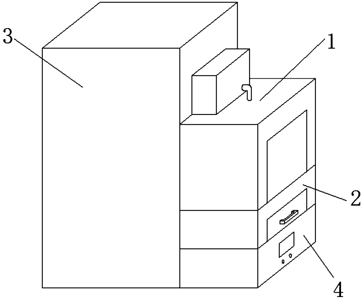
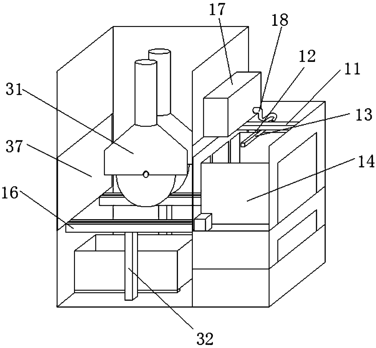
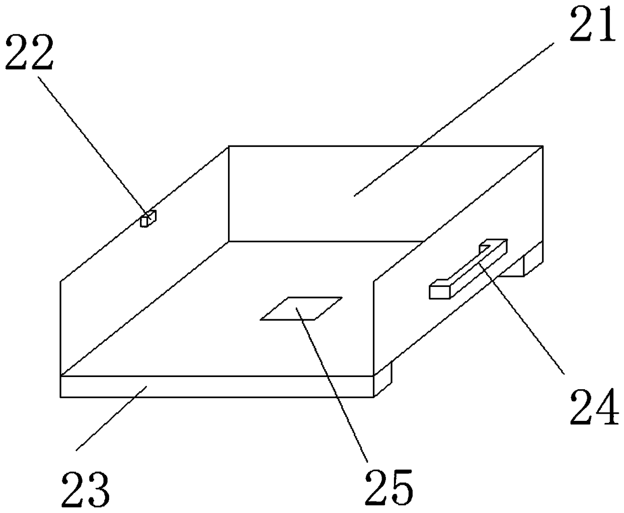
[0025] Such as Figure 1-7As shown, a waste PCB board processing device includes a removal bin 1, an electronic component collection bin 2, a cutting bin 3 and a control box 4, the electronic component collection bin 2 is located above the control box 4, and the disassembly bin 1 is located at the electronic Above the component collection bin 2, the cutting bin 3 is located on ...


PUM


Abstract

The invention provides a waste PCB treatment device which comprises a removal bin, an electronic component collecting bin, a cutting bin and a control box. The dismounting bin comprises a first sliding track, a first sliding block, an air knife, a dismounting box, a second sliding block, a second sliding track, a hot air device and a connecting pipeline. The dismounting box comprises a box body, amovable plate, a motor and a rotating shaft. The electronic component collecting bin comprises a first collecting box, a first sensor, a third sliding track, a first handle and a third sensor. The cutting bin comprises a cutting device, a supporting rod, a second collecting box, a second sensor, a fourth sliding track, a second handle and an opening. The control box comprises a control panel, a first warning lamp, a second warning lamp, an electricity storage device and a controller. According to the waste PCB treatment device, the functions of automatically dismounting and cutting a waste PCB are achieved, electronic components and the PCB are automatically classified and recycled, and the waste PCB treatment device is simple in structure, more automatic and more intelligent.

Description

Technical field: [0001] The invention relates to the technical field of recycling and processing of waste PCB boards, in particular to a device for recycling and processing waste and old PCB boards. Background technique: [0002] With the development of society and the continuous improvement of living standards, the consumption of electronic products continues to increase, and the replacement rate and elimination rate of household appliances are also rising. The household appliances that are updated every year include TVs, washing machines, refrigerators, air conditioners, computers and other small appliances. The quantity is increasing year by year, but the disposal of printed circuit boards in these waste electrical appliances, the reduction of environmental pollution and the reuse of resources have become a very substantial issue. [0003] The PCB board is a collection of glass fiber, resin, copper and tin. The metal content in the PCB board is about 40%. For the ever-inc...

Claims


Application Information

Patent Timeline
IPC IPC(8): B09B3/00B09B5/00B26D1/15
CPCB09B3/00B09B5/00B26D1/15B09B3/40Y02W30/82
Inventor 陈美金
Owner HUZHOU HUINENG ELECTROMECHANICAL TECH CO LTD
Why Eureka
Try Eureka