
OLED display panel, and backboard laminating method and device

A technology for display panels and backplanes, applied in photovoltaic power generation, electrical components, electric solid devices, etc., can solve the problems of OLED panel breakage, generation of air bubbles, and uneven surface of OLED panels, so as to ensure smoothness and avoid air bubbles , height and movement speed are easy to control

Active Publication Date: 2018-11-13
WUHAN CHINA STAR OPTOELECTRONICS SEMICON DISPLAY TECH CO LTD
View PDF4 Cites 3 Cited by
  • Summary
  • Abstract
  • Description
  • Claims
  • Application Information

AI Technical Summary

Problems solved by technology

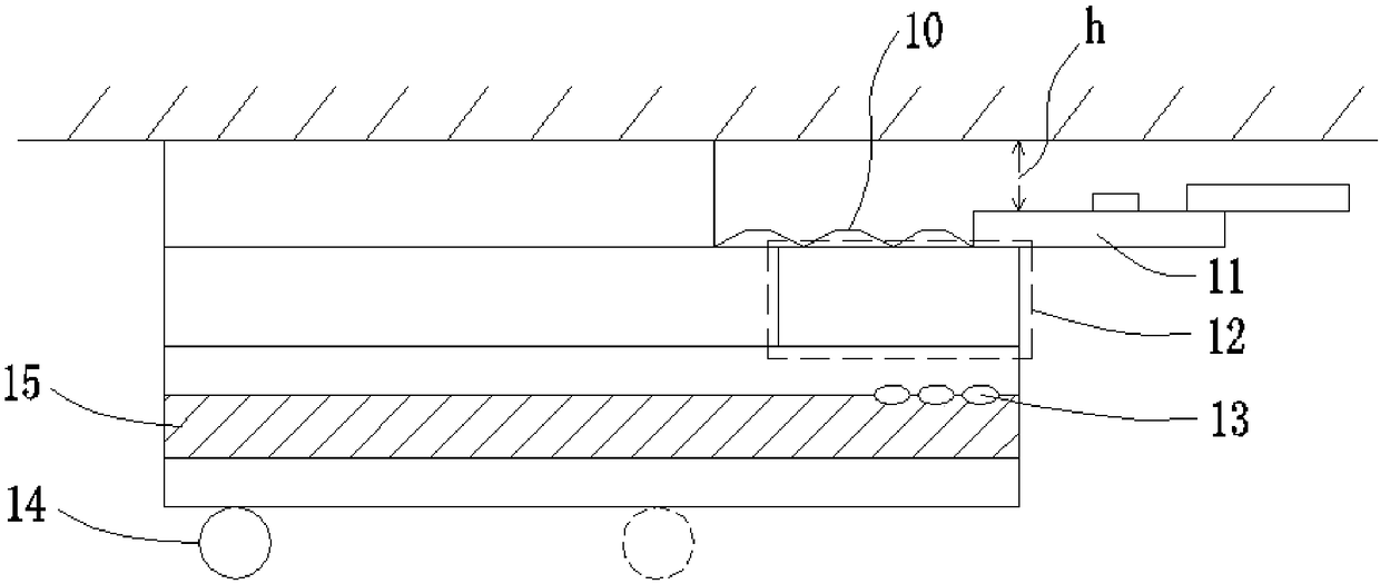
However, for the current technology, the main problem is the bubble problem during the backplane attachment process on the side of the OLED panel binding area, such as figure 1 As shown: in the OLED panel manufacturing process, due to the height difference h between the side of the OLED panel bound with the Chip On FPC (COF) and the overall height of the OLED panel, the backplane 15 is attached to During the attaching process, the roller 14 cannot be rolled to the corresponding position corresponding to the binding area 12, otherwise the OLED panel corresponding to the binding area 12 will be broken, resulting in damage to the OLED panel
If the roller 14 is not rolled to the corresponding position corresponding to the binding area 12, it will cause the generation of air bubbles 13 when the back plate 15 is attached corresponding to the binding area 12, and the existence of the air bubbles 13 will cause Affects efficiency and yield throughout the manufacturing process
Secondly, due to the existence of colloid 10 above the binding area 12 of the OLED panel, the surface of the OLED panel at the binding area 12 is uneven, so it is difficult to solve the problem by the design of the fixture.

Method used


Image

  • OLED display panel, and backboard laminating method and device
  • OLED display panel, and backboard laminating method and device
  • OLED display panel, and backboard laminating method and device

Examples


Embodiment Construction

[0041] The technical solutions in the embodiments of the present invention will be clearly and completely described below in conjunction with the drawings in the embodiments of the present invention. Obviously, the described embodiments are only a part of the embodiments of the present invention, rather than all the embodiments. Based on the embodiments of the present invention, all other embodiments obtained by those skilled in the art without creative work shall fall within the protection scope of the present invention.

[0042] The present invention is directed to the prior art method and device for attaching the backplane of the OLED display panel. Since bubbles are easily generated when the backplane is attached, the product efficiency and yield are affected, and the OLED display panel is easily affected during attachment. This embodiment can solve the technical problem of damage.

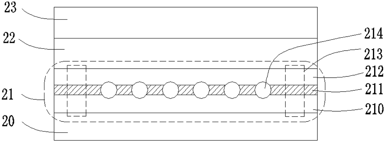
[0043] Refer to figure 2 , figure 2 It is a schematic diagram of the structure of an OLED di...


PUM


Abstract

The invention provides an OLED display panel, and a backboard laminating method and device. The OLED display panel comprises a flexible substrate, a thin film transistor layer, and a light emitting layer, wherein the flexible substrate comprises a cutting area for a subsequent cutting process; the thin film transistor layer is prepared on the flexible substrate; the light emitting layer is prepared on the thin film transistor layer; the flexible substrate comprises a first flexible substrate layer, a fixed layer and a second flexible substrate layer which are stacked in sequence; the thin filmtransistor layer is positioned on the second flexible substrate layer, wherein the fixed layer comprises an organic film layer and magnetic particles embedded in the organic film layer; the diameterof the magnetic particles is smaller than the thickness of the flexible substrate; and the magnetic particles are positioned in the flexible substrate.

Description

Technical field [0001] The invention relates to the technical field of display panel manufacturing, in particular to a method and device for attaching an OLED display panel and a backplane. Background technique [0002] OLED has a series of advantages such as flexibility, self-luminescence, fast response rate, high contrast, etc., gradually replacing LCD and becoming the most promising display of the next generation. In the production process of OLED panels, the yield and efficiency of module sites have an important impact on the quality and mass production rate of OLED panels. [0003] In the current module process, the backplane attachment (BP Lami) is one of the important process points, and the backplane mainly provides a certain support for the entire OLED panel. However, for the current technology, the main problem is the bubble problem during the attachment process of the backplane on the side of the OLED panel binding area, such as figure 1 As shown: during the production ...

Claims


Application Information

Patent Timeline
Patent Type & Authority Applications(China)
IPC IPC(8): H01L27/32H01L51/52H01L51/56
CPCH10K59/12H10K77/111H10K50/80H10K71/00Y02E10/549
Inventor 包潘飞
Owner WUHAN CHINA STAR OPTOELECTRONICS SEMICON DISPLAY TECH CO LTD
Learn More