Leakage test method

A test method, a technology to be tested, applied in circuits, semiconductor/solid-state device testing/measurement, electrical components, etc., can solve problems such as loss of metal wires, damage to the surface of samples, and the impact of failure analysis

Active Publication Date: 2020-10-23
YANGTZE MEMORY TECH CO LTD
View PDF6 Cites 0 Cited by
  • Summary
  • Abstract
  • Description
  • Claims
  • Application Information

AI Technical Summary

Problems solved by technology

During the detection process, the surface of the sample needs to be ground to a place close to the surface of the metal layer to be tested, so that the metal wire of the sample loses the protection of the surface oxide layer. This method will damage the surface of the sample and have an adverse effect on the subsequent failure analysis.

Method used


Image

  • Leakage test method
  • Leakage test method
  • Leakage test method

Examples


Embodiment Construction

[0018] The specific implementation of the leakage test method provided by the present invention will be described in detail below in conjunction with the accompanying drawings.

[0019] Please refer to Figure 1 to Figure 4 , is a structural schematic diagram of a leakage test process according to a specific embodiment of the present invention.

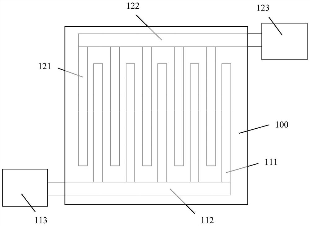
[0020] Please refer to figure 1 , providing a sample to be tested, figure 1 is a top perspective view of the sample to be tested.

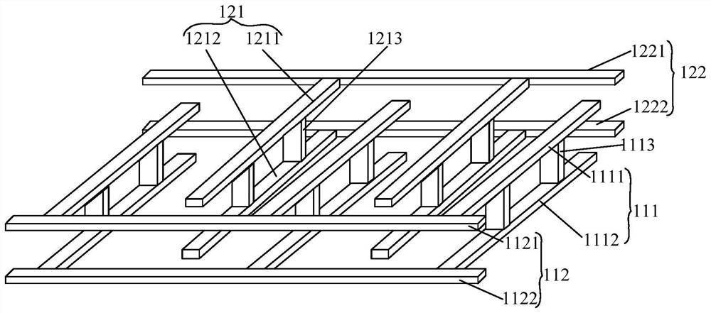
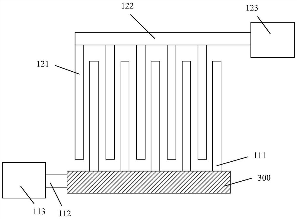
[0021] The sample to be tested includes an insulating layer 100, and a leakage test structure is formed in the insulating layer 100. The leakage test structure includes: a first comb-shaped metal wire, a second comb-shaped metal wire, and the first comb-shaped metal wire The line includes a plurality of first comb-toothed metal lines 111 arranged in parallel, and the second comb-shaped metal line includes a plurality of second comb-toothed metal lines 121 arranged in parallel, and the first comb-tooth...


PUM


Abstract

The invention relates to an electric leakage test method, which comprises the steps of providing a test sample, wherein the test sample includes an insulating layer, the insulating layer is internallyprovided with an electric leakage test structure, the electric leakage test structure includes a first comb-shaped metal wire and a second comb-shaped metal wire, the first comb-shaped metal wire includes a plurality of first comb tooth metal wires which are arranged in parallel, the second comb-shaped metal wire includes a plurality of second comb tooth metal wires which are arranged in parallel, and the first comb tooth metal wires and the second comb tooth metal wires are arranged in a mutually parallel manner at intervals; etching the test sample, and forming a groove in the test sample,wherein the side wall at one side of the groove at least exposes end parts of the plurality of first comb tooth metal wires; and positioning failure location through observing the voltage contrast atthe end parts of the plurality of first comb tooth metal wires exposed by the side wall of the groove. The failure location can be positioned without destroying the surface of the test sample according to the method.

Description

technical field [0001] The invention relates to the technical field of semiconductors, in particular to a leakage test method. Background technique [0002] Integrated circuit manufacturing technology is a complicated process, and the technology is updated very quickly. A key parameter that characterizes integrated circuit manufacturing technology is the minimum feature size, that is, critical dimension (CD). With the continuous development of semiconductor technology, the critical dimension of devices is getting smaller and smaller, and the distance between devices is getting smaller and smaller. Small. Two. Any abnormality in the semiconductor manufacturing process will lead to short circuit or leakage between components, so the leakage between components on the semiconductor chip becomes an item that must be strictly monitored. [0003] In the manufacture of semiconductor devices, a multilayer metal interconnection structure is usually used to electrically connect vario...

Claims


Application Information

Patent Timeline
Patent Type & Authority Patents(China)
IPC IPC(8): H01L21/66
CPCH01L22/14
Inventor 费腾李桂花蔚倩倩杜晓琼仝金雨
Owner YANGTZE MEMORY TECH CO LTD
Why Eureka
Try Eureka