A light-emitting diode epitaxial wafer and its preparation method

A technology for light-emitting diodes and epitaxial wafers, applied in semiconductor devices, electrical components, circuits, etc., can solve the problems of reducing the overall quality of epitaxial wafers, affecting the luminous efficiency of light-emitting diodes, etc., to reduce the formation of non-radiative recombination centers and improve luminous efficiency. , Improve the effect of luminous efficiency

Active Publication Date: 2020-04-07
HC SEMITEK SUZHOU
View PDF3 Cites 0 Cited by
  • Summary
  • Abstract
  • Description
  • Claims
  • Application Information

AI Technical Summary

Problems solved by technology

However, during the growth process of the undoped GaN layer, compressive stress will continue to accumulate in the undoped GaN layer, and the compressive stress will form line defects in the undoped GaN layer and bring about piezoelectric polarization, thereby reducing the The overall quality of the epitaxial wafer affects the luminous efficiency of the light-emitting diode produced from the epitaxial wafer

Method used


Image

  • A light-emitting diode epitaxial wafer and its preparation method
  • A light-emitting diode epitaxial wafer and its preparation method
  • A light-emitting diode epitaxial wafer and its preparation method

Examples


Embodiment Construction

[0029] In order to make the object, technical solution and advantages of the present invention clearer, the implementation manner of the present invention will be further described in detail below in conjunction with the accompanying drawings.

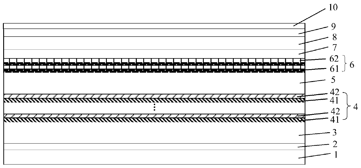
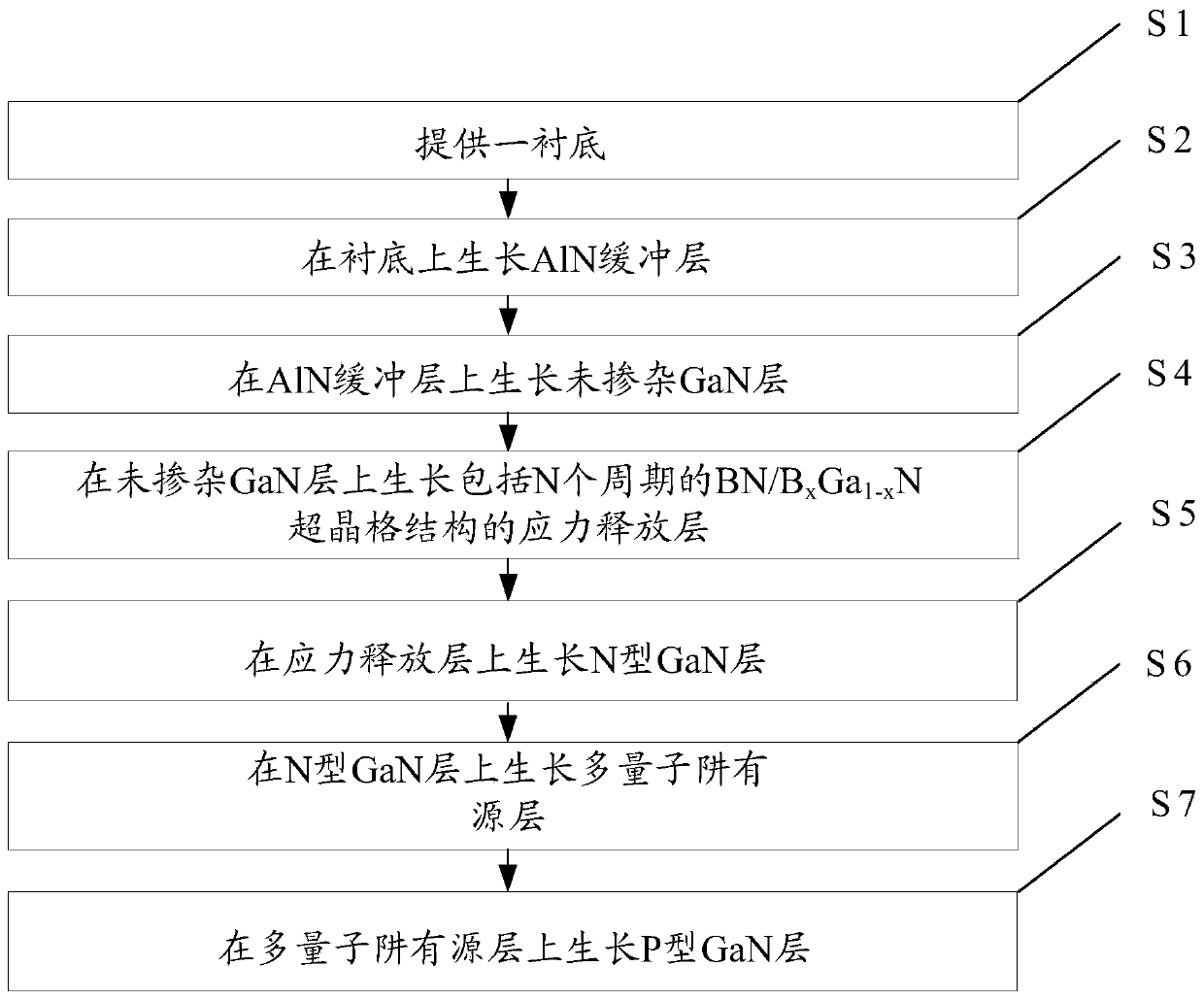
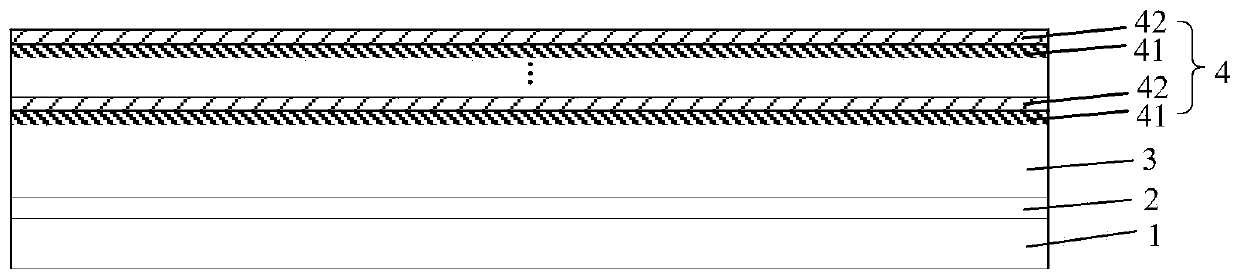
[0030] figure 1 It is a schematic structural diagram of a light-emitting diode epitaxial wafer provided by an embodiment of the present invention, as shown in figure 1 As shown, the epitaxial wafer includes a substrate 1 and an AlN buffer layer 2, an undoped GaN layer 3, a stress release layer 4, an N-type GaN layer 5, and a multi-quantum well active layer 6 stacked on the substrate 1 in sequence. and a P-type GaN layer 7, wherein the stress release layer 4 includes N periods of BN / B x Ga 1-x N superlattice structure, 0.01

[0031] Set BN / B including N periods on the undoped GaN layer x Ga 1-x Stress release layer with N superlattice structure, BN / B x Ga 1-x The N superlattice structure wi...


PUM

PropertyMeasurementUnit
thicknessaaaaaaaaaa
thicknessaaaaaaaaaa
temperatureaaaaaaaaaa

Abstract

The invention discloses an LED epitaxial wafer and a preparation method thereof, and belongs to the semiconductor photoelectric field. A non-doped GaN layer is provided a stress release layer including N periods of BN / BxGa1-xN superlattice structures, the BN / BxGa1-xN superlattice structures accumulate a tension in an epitaxial layer, the tension can offset part of a crushing stress in non-doped GaN, and further linear defect and piezoelectric polarization caused by the crushing stress in the non-doped GaN can be reduced. Reduction of the line defects in the epitaxial wafer can improve the quality of the epitaxial wafer, and reduce formation of non-radiation composite centers in a multi-quantum well active region greatly, and further, the light emitting efficiency can be improved. Reductionof piezoelectric polarization can reduce a quantum well Stark restriction effect caused by piezoelectric polarization and spontaneous polarization in the epitaxial wafer, and the light emitting efficiency is improved further.

Description

technical field [0001] The invention relates to the field of semiconductor optoelectronics, in particular to a light-emitting diode epitaxial wafer and a preparation method thereof. Background technique [0002] The epitaxial wafer is the basic structure for making light-emitting diodes. The structure of the epitaxial wafer includes a substrate and an epitaxial layer grown on the substrate. Among them, the structure of the epitaxial layer mainly includes: AlN buffer layer, undoped GaN layer, N-type GaN layer, multi-quantum well active layer and P-type GaN layer grown on the substrate in sequence. [0003] The setting of the undoped GaN layer can reduce the lattice mismatch existing between the N-type GaN layer and the substrate, so as to improve the growth quality of the epitaxial layer grown after the undoped GaN layer. However, during the growth process of the undoped GaN layer, compressive stress will continue to accumulate in the undoped GaN layer, and the compressive s...

Claims


Application Information

Patent Timeline
Patent Type & Authority Patents(China)
IPC IPC(8): H01L33/04H01L33/12H01L33/00
CPCH01L33/007H01L33/04H01L33/12
Inventor 陶章峰乔楠余雪平程金连胡加辉
Owner HC SEMITEK SUZHOU
Why Eureka
Try Eureka