Optical lattice imaging device

An imaging device and optical crystal technology, which is applied in measuring devices, fluorescence/phosphorescence, and material analysis through optical means, can solve problems that are difficult to achieve, and achieve the effects of small distortion, accurate measurement, and large axial magnification

Inactive Publication Date: 2018-11-23
NAT TIME SERVICE CENT CHINESE ACAD OF SCI
View PDF9 Cites 4 Cited by
  • Summary
  • Abstract
  • Description
  • Claims
  • Application Information

AI Technical Summary

Problems solved by technology

In particular, sometimes it is necessary to see how the shape of the atomic group in the crystal lattice ...

Method used


Image

  • Optical lattice imaging device
  • Optical lattice imaging device
  • Optical lattice imaging device

Examples


Embodiment 1

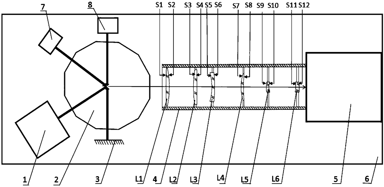
[0036] exist figure 1 In the optical lattice imaging device of the present invention, an atomic source 1, a vacuum device 2, a zero-degree high mirror 3, a lens barrel 4, a CCD imaging device 5, and a detection laser 7 are fixedly connected on the mounting plate with threaded fasteners , lattice light laser 8, atom source 1, vacuum device 2, zero-degree high mirror 3, lens barrel 4, CCD imaging device 5, detection laser 7, and lattice light laser 8 are in the same plane, and vacuum device 2 is installed on the atom In the light emission direction of the source 1, the probe laser 7, and the lattice laser 8, the zero-degree high mirror 3 is installed directly opposite the lattice laser 8. In this embodiment, the atoms in the atom source 1 are 87 Sr atoms, after a series of cooling, the atoms generated by the atomic source produce cold atomic groups with a temperature in the uK level in the center of the vacuum device 2, and the lattice laser 8 outputs a Gaussian beam with a wave...


PUM

PropertyMeasurementUnit
Surface curvatureaaaaaaaaaa
Refractive indexaaaaaaaaaa

Abstract

The invention relates to an optical lattice imaging device. An atom source, a vacuum unit, a zero high-reflectivity mirror, a lens cone, a CCD imaging device, a detecting laser and a lattice light laser are arranged on a mounting plate; the vacuum unit is arranged on a light emitting direction of the atom source, the detecting laser and the lattice light laser; the zero high-reflectivity mirror isarranged on the front surface of the lattice light laser; the center lines of the lens cone and the CCD imaging device are coincided with each other and vertical to the propagation direction of lattice light; a lens assembly is arranged in the lens cone; the lens assembly comprises a convex lens, a plano-convex lens, a concave mirror, a first meniscus lens, a second meniscus lens and a plano-concave lens in turn from left to right. A larger caliber is adopted by the optical lattice imaging device, so that the collecting efficiency of fluorescent light can be increased, the spatial resolutionis larger, the CCD resolution ratio can be fully utilized, the distortion is smaller, the experimental error is reduced and the device can be popularized and applied to the field of optical lattice imaging devices.

Description

technical field [0001] The invention belongs to the technical field of optical devices, and in particular relates to a lens device for imaging atomic groups loaded in an optical lattice. Background technique [0002] In the research process of most cold atom experiments and optical lattice clocks, atoms are required to be loaded in the optical lattice, so as to eliminate the Doppler effect and photon recoil frequency shift and greatly reduce the collision between atoms. Optical lattice loading is almost a must in studies of precision atomic spectroscopy, Bose-Einstein condensates, and optical lattice atomic clocks. [0003] The optical lattice means that a Gaussian beam is converged and injected into the vacuum cavity, and then the beam is returned to the original path by a mirror. The incident light and the reflected light need to be completely coincident, especially the positions of the beam waists of the two must coincide. In this way, the incident light and the reflecte...

Claims


Application Information

Patent Timeline
IPC IPC(8): G01N21/64
CPCG01N21/6404
Inventor 卢晓同常宏
Owner NAT TIME SERVICE CENT CHINESE ACAD OF SCI
Why Eureka
Try Eureka