Chip on film package

A chip-on-film and package technology, applied in the field of chip-on-film packages, can solve problems such as limiting integrated circuits and chip space.

Inactive Publication Date: 2018-11-23
NOVATEK MICROELECTRONICS CORP
View PDF5 Cites 0 Cited by
  • Summary
  • Abstract
  • Description
  • Claims
  • Application Information

AI Technical Summary

Problems solved by technology

However, when COF packages are combined with other functions (such as touch panels) or applied in small or medium-sized panels, more and more electromagnetic interference between various integrated circuits and chips is observed, thus limiting the available for assembly. and space for installing integrated circuits and chips

Method used


Image

  • Chip on film package
  • Chip on film package
  • Chip on film package

Examples


Embodiment Construction

[0079] Reference will now be made in detail to the presently preferred embodiments of the invention, examples of which are illustrated in the accompanying drawings. Wherever possible, the same reference numbers will be used in the drawings and description to refer to the same or like parts.

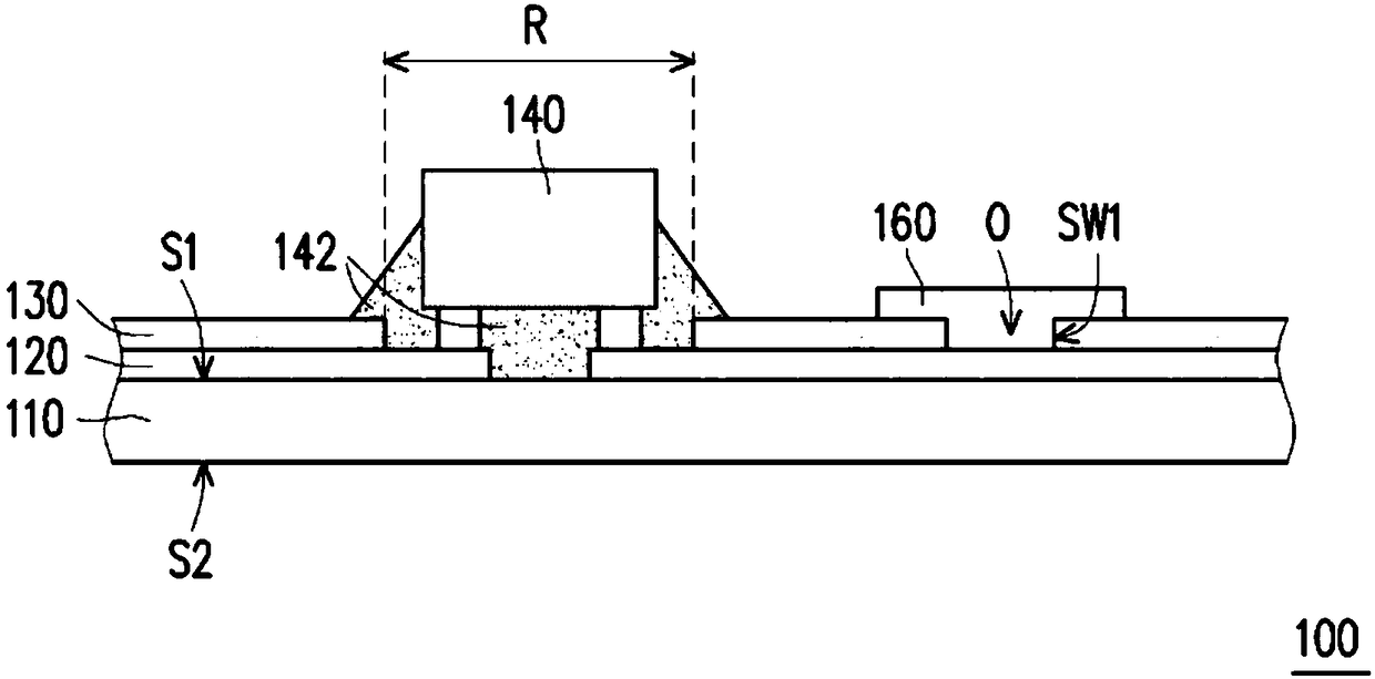
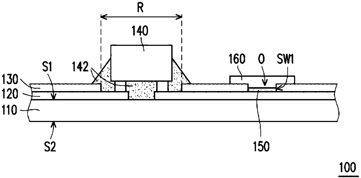
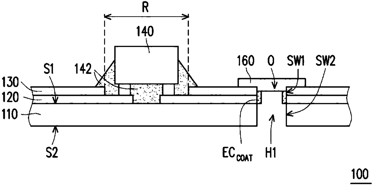
[0080] Figures 1A to 1E Each is a cross-sectional view of a chip-on-film package according to an embodiment of the present invention. Figure 2A to Figure 2B are top views of chip-on-film packages according to embodiments of the present invention, respectively. It should be noted that Figure 1A to Figure 1E each of which is Figure 2A to Figure 2B A cross-sectional view of either one along line A-A'.

[0081] refer to Figure 1A , in this embodiment, the chip-on-film package 100 includes a base film 110 , a patterned circuit layer 120 , a first solder resist layer 130 , a chip 140 and a first conductive film 160 . The base film 110 includes a first surface S1 and a mounting region ...


PUM


Abstract

The invention discloses a chip on film package, which includes a base film, a patterned circuit layer, a solder resist layer, a chip and a first conductive film. The base film includes a first surfaceand a mounting region located on the first surface. The patterned circuit layer is disposed on the first surface. The solder resist layer partially covers the patterned circuit layer. The chip is disposed in the mounting region and electrically connected to the patterned circuit layer. The first conductive film covers at least a part of the first solder resist layer and an opening exposing at least a part of the patterned circuit layer, wherein the first conductive film is configured to shield electromagnetic interference (EMI) emanating from the chip and is electrically connected to the patterned circuit layer.

Description

technical field [0001] The invention relates to a chip package. More specifically, the present invention relates to a chip-on-film package. Background technique [0002] In semiconductor production, the manufacture of integrated circuits (integrated circuits, ICs) can be divided into three different stages, namely, the chip fabrication stage, the integrated circuit fabrication stage, and the IC packaging stage (such as the application of chip-on-film (COF ) packages). [0003] Conventionally, there is no measure for shielding electromagnetic interference (EMI) for COF packages. However, when COF packages are combined with other functions (such as touch panels) or applied in small or medium-sized panels, more and more electromagnetic interference between various integrated circuits and chips is observed, thus limiting the available for assembly. And the space to install integrated circuits and chips. Contents of the invention [0004] It is therefore an object of the pr...

Claims


Application Information

Patent Timeline
Patent Type & Authority Applications(China)
IPC IPC(8): H01L23/31H01L23/495H01L23/60
CPCH01L23/3121H01L23/49579H01L23/60H01L2224/16225H01L2224/32225H01L2224/73204H01L2924/3025H01L23/552H01L2224/92125H01L2924/15151H01L2924/15192H01L23/49827H01L2924/00
Inventor 黄文静林泰宏
Owner NOVATEK MICROELECTRONICS CORP
Why Eureka
Try Eureka