Power packaging structure and lead frame thereof

A packaging structure and lead frame technology, applied in electrical components, electrical solid devices, circuits, etc., can solve the problems of large product size and large lead frame area, and achieve the effect of reducing product size, large contact area, and increasing the number of products.

Pending Publication Date: 2018-11-23
HANGZHOU SILAN MICROELECTRONICS
View PDF0 Cites 0 Cited by
  • Summary
  • Abstract
  • Description
  • Claims
  • Application Information

AI Technical Summary

Problems solved by technology

If only the cross-sectional area of ​​the current channel is considered, the contact surface area of...

Method used


Image

  • Power packaging structure and lead frame thereof
  • Power packaging structure and lead frame thereof
  • Power packaging structure and lead frame thereof

Examples


Embodiment Construction

[0042] Hereinafter, the present invention will be described in more detail with reference to the accompanying drawings. In the various figures, identical elements are indicated with similar reference numerals. For the sake of clarity, various parts in the drawings have not been drawn to scale. Also, some well-known parts may not be shown.

[0043] In the following, many specific details of the present invention are described, such as device structures, materials, dimensions, processing techniques and techniques, for a clearer understanding of the present invention. However, the invention may be practiced without these specific details, as will be understood by those skilled in the art.

[0044] The invention can be embodied in various forms, some examples of which are described below.

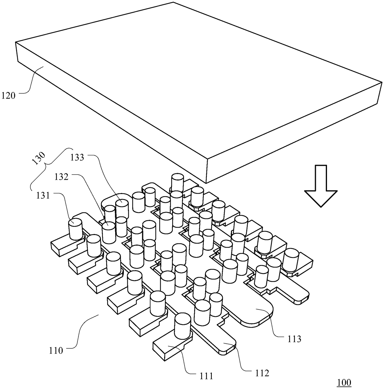
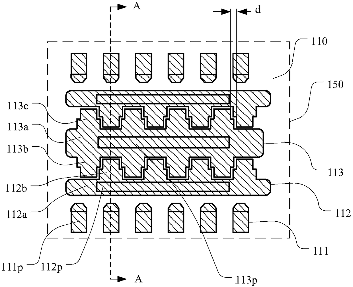
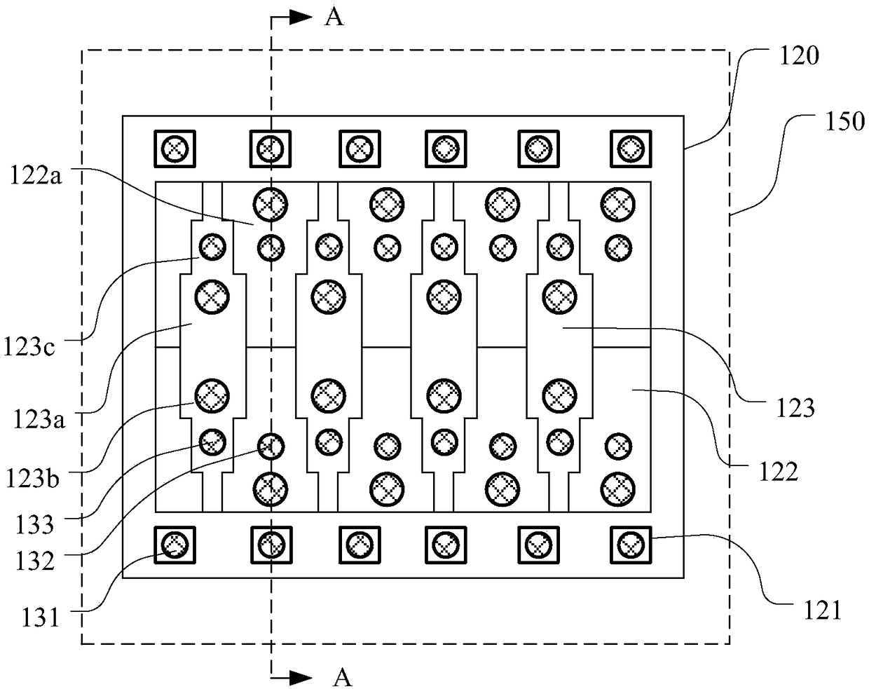
[0045] figure 1 An internal perspective view of the power package package structure according to the first embodiment of the present invention is shown.

[0046] As shown in the figure, th...


PUM


Abstract

The invention discloses a power packaging structure and a lead frame thereof. The lead frame comprises a first set of pins and a second set of pins. A first surface of the first set of pins provides afirst contact surface for an internal electrical connection. The first surface of the second set of pins provides a second contact surface for the internal electrical connection, and the second set of pins respectively comprise a conductive strip and a plurality of protrusions extending on at least one side edge of the conductive strip, wherein the width direction of the plurality of protrusionsis parallel to the side edge of the conductive strip, and the width of the plurality of protrusions varies with the distance from the side edges of the conductive strip. According to the power packaging structure and the lead frame thereof, the lead frame in the power packaging structure provides a contact surface in electrical connection with a set of conductive posts using the protrusion of pinto improve current carrying capability and reduce the size of product.

Description

technical field [0001] The present invention relates to the technical field of integrated semiconductors, more specifically, to a power packaging structure and its lead frame. Background technique [0002] In consumer electronic products, such as chargers, LCD TVs, medical electronics and other equipment, products with power packaging structures, such as high-current DC-DC converters, are widely used. The main performance parameters of power package structure products include high current and low power consumption. In order to achieve low power consumption, a small internal resistance on the current path is required. The internal resistance of power packaging structure products includes not only the on-resistance of active components in the chip, but also the contact resistance and wiring resistance introduced in the packaging structure. Therefore, the packaging structure adopted by power packaging structure products is also the main factor affecting performance parameters...

Claims


Application Information

Patent Timeline
IPC IPC(8): H01L23/495
CPCH01L23/4952H01L2224/14H01L2224/16245H01L2224/17
Inventor 刘静张秀梅宁志华
Owner HANGZHOU SILAN MICROELECTRONICS
Why Eureka
Try Eureka