Semiconductor device and manufacturing method thereof

A manufacturing method and semiconductor technology, applied in the direction of semiconductor/solid-state device manufacturing, semiconductor devices, transistors, etc., can solve the problems of small current, increase cost, increase the size of junction field effect transistor, etc., and achieve the effect of high current

Active Publication Date: 2018-11-23
VANGUARD INTERNATIONAL SEMICONDUCTOR CORPORATION
View PDF10 Cites 0 Cited by
  • Summary
  • Abstract
  • Description
  • Claims
  • Application Information

AI Technical Summary

Problems solved by technology

However, JFETs can only supply small currents
When there is a demand for high current, often only

Method used


Image

  • Semiconductor device and manufacturing method thereof
  • Semiconductor device and manufacturing method thereof
  • Semiconductor device and manufacturing method thereof

Examples


Example Embodiment

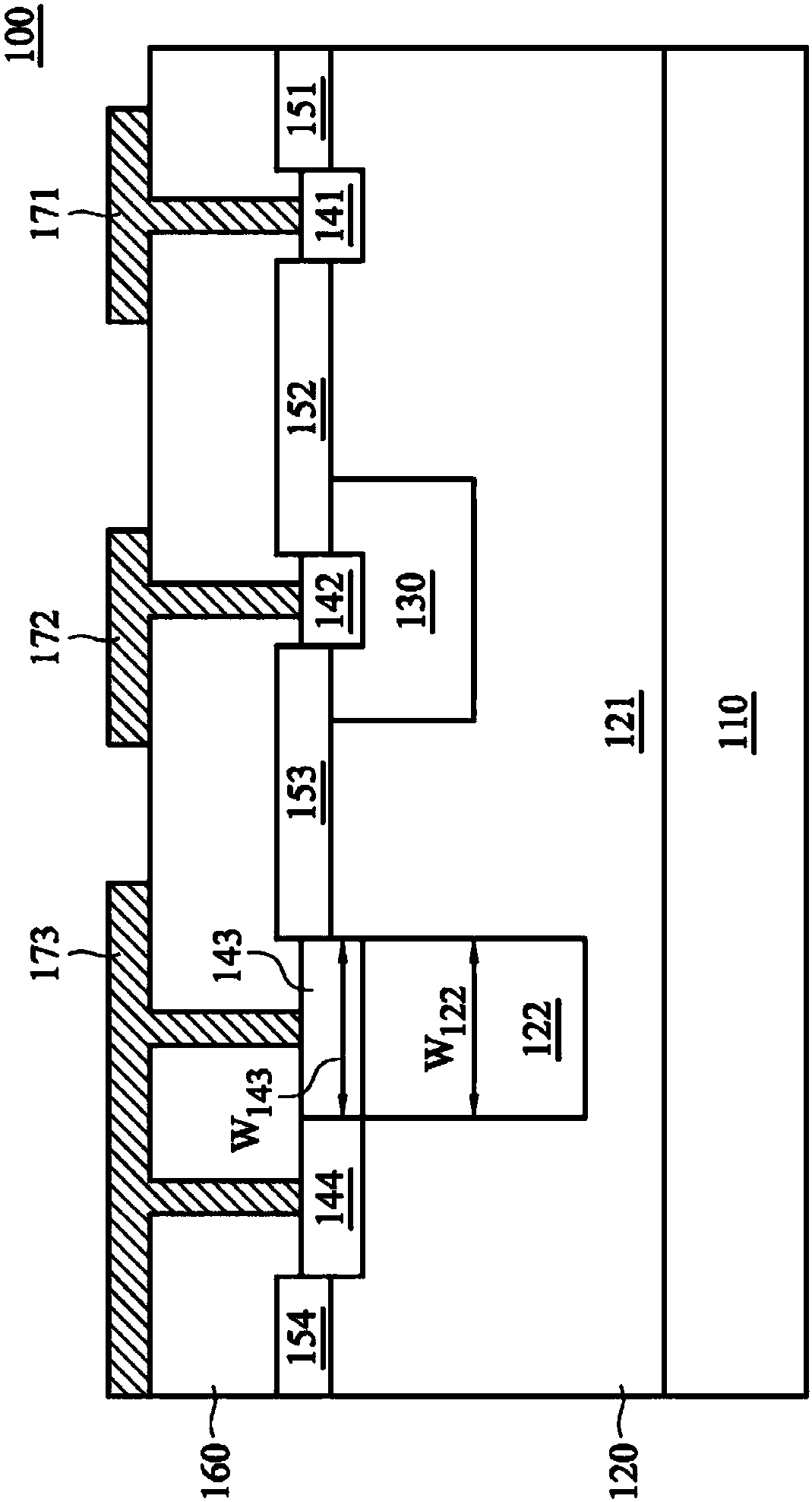
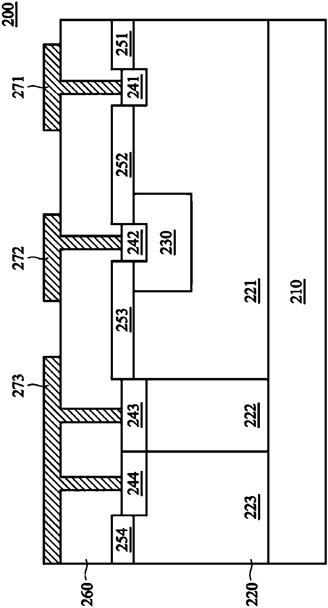
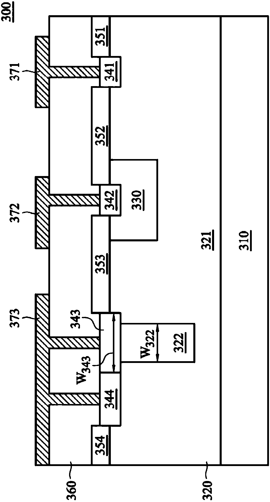
[0021] In order to make the purpose, features and advantages of the present invention more comprehensible, embodiments are specifically listed below, in conjunction with the accompanying drawings, for detailed description. The specification of the present invention provides different examples to illustrate the technical features of different embodiments of the present invention. Wherein, the configuration of each element in the embodiment is for illustrative purposes and is not used to limit the present invention. In addition, in the embodiments, the part of the symbols of the drawings is repeated, in order to simplify the description, it does not mean the correlation between the different embodiments.

[0022] Here, the terms "about" and "approximately" usually mean within 20% of a given value or range, preferably within 10%, and more preferably within 5%. The quantity given here is an approximate quantity, which means that the meaning of "about" and "approximately" can still b...


PUM


Abstract

The invention proposes a semiconductor device and a manufacturing method thereof. The semiconductor device comprises a semiconductor substrate, a first well, a second well, a first doping region, a second doping region, a third doping region and a fourth doping region, wherein the semiconductor substrate has a first conductive type, the first well is formed in the semiconductor substrate and has asecond conductive type, the first well is provided with a first region and a second region, the doping concentration of the first region is higher the the doping concentration of the second region, the second well has the first conductive type and is formed in the first region, the first doping region has the second conductive type and is formed in the first region, the second conductive type isdifferent from the first conductive type, the second doping region has the first conductive type and is formed in the second well, the third doping region has the first conductive type and is formed in the second region, and the fourth doping region has the second conductive type and is formed in the first region.

Description

technical field [0001] The present invention relates to a semiconductor device, in particular to a semiconductor device with a PN junction. Background technique [0002] Transistors are mainly classified into bipolar junction transistors (bipolar junction transistors; BJT) and field effect transistors (field effect transistors; FETs). Because the structure of the field effect transistor is simpler than that of the bipolar junction transistor, it is often used. Field effect transistors are further divided into metal oxide semiconductor field effect transistors (metal oxide semiconductor FETs; MOSFETs) and junction field effect transistors (junction FETs; JFETs). However, JFETs can only supply small currents. When there is a demand for a large current, it is often only possible to increase the size of the junction field effect transistor, but it will increase the cost. Contents of the invention [0003] The present invention provides a semiconductor device, comprising a s...

Claims


Application Information

Patent Timeline
IPC IPC(8): H01L29/36H01L21/337H01L29/80
CPCH01L29/36H01L29/66893H01L29/80
Inventor 林文新林鑫成吴政璁胡钰豪
Owner VANGUARD INTERNATIONAL SEMICONDUCTOR CORPORATION
Why Eureka
Try Eureka