Semiconductor field effect transistor and preparation method thereof

A technology of field effect transistors and transistors, applied in the field of communication, can solve problems such as large switching loss, poor heat dissipation, and small breakdown voltage

Inactive Publication Date: 2018-11-27
SHENZHEN UNIV
View PDF3 Cites 1 Cited by
  • Summary
  • Abstract
  • Description
  • Claims
  • Application Information

AI Technical Summary

Problems solved by technology

[0003] The main purpose of the present invention is to provide a semiconductor field effect transistor and its preparation method, aiming to solve the probl

Method used


Image

  • Semiconductor field effect transistor and preparation method thereof
  • Semiconductor field effect transistor and preparation method thereof

Examples


Embodiment Construction

[0021] In order to make the purpose, features and advantages of the present invention more obvious and understandable, the technical solutions in the embodiments of the present invention will be clearly and completely described below in conjunction with the accompanying drawings in the embodiments of the present invention. Obviously, the described The embodiments are only some of the embodiments of the present invention, but not all of them. Based on the embodiments of the present invention, all other embodiments obtained by those skilled in the art without making creative efforts belong to the protection scope of the present invention.

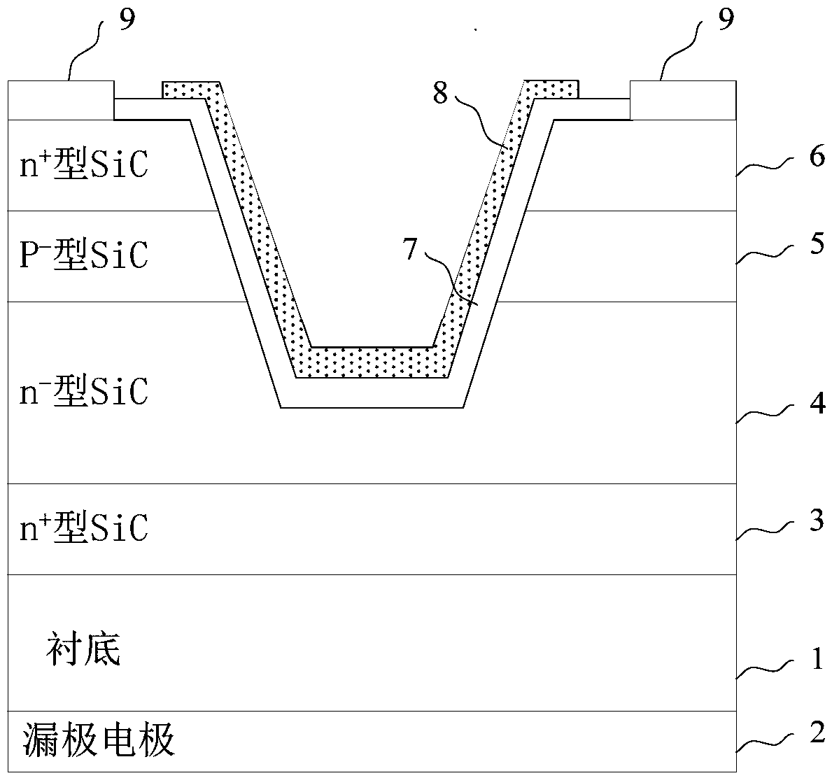
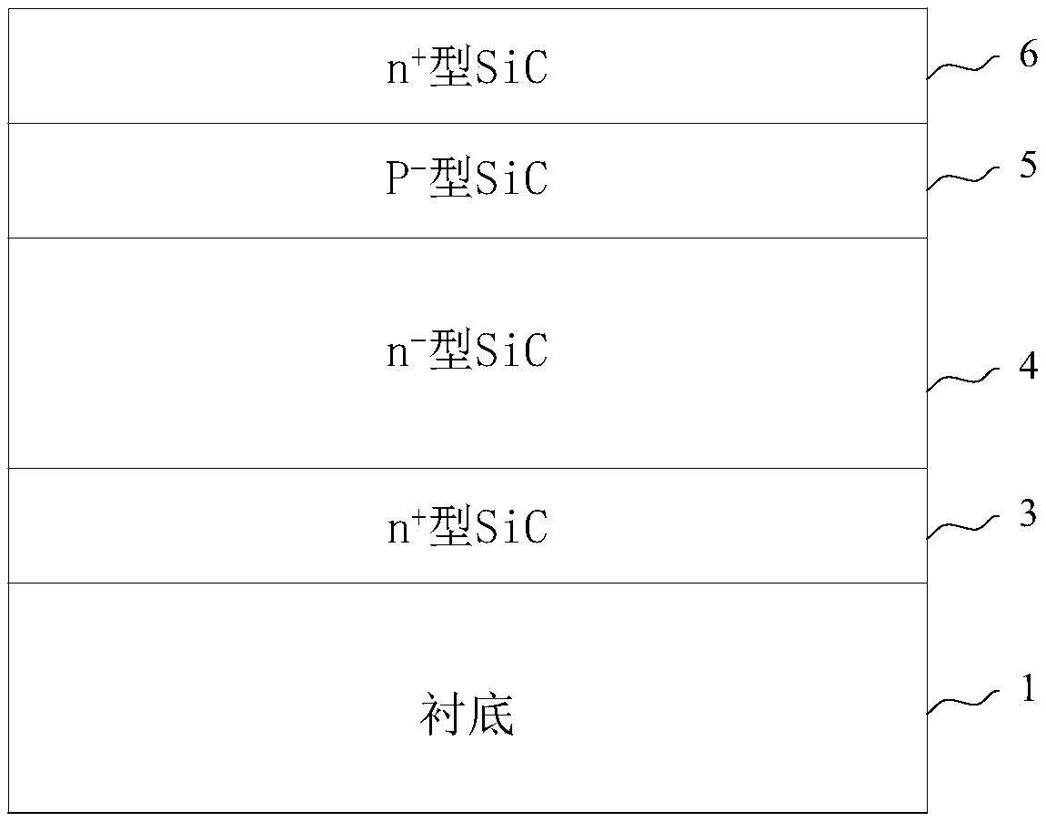
[0022] figure 1 A schematic structural diagram of a semiconductor field effect transistor provided for this embodiment, the transistor includes: a substrate (1), a drain electrode (2) below the substrate, and a drain electrode (2) placed vertically above the substrate in sequence away from the substrate no + Type SiC(3), n - Type SiC(4), P...


PUM

PropertyMeasurementUnit
Thicknessaaaaaaaaaa
Thicknessaaaaaaaaaa
Thicknessaaaaaaaaaa

Abstract

The invention discloses a semiconductor field effect transistor and a preparation method thereof. The semiconductor field effect transistor comprises a substrate, a drain electrode, n<+> type SiC, n<-> type SiC, P<-> type SiC and n<+> type SiC, wherein the n<+> type SiC, the n<-> type SiC, the P<-> type SiC and the n<+> type SiC are sequentially and vertically arranged on the substrate in a direction far away from the substrate direction; the transistor is provided with an inverted trapezoidal groove deposited with a Si<x>N<y>-SiO2 double-layer structure; a grid electrode and a source electrode contact electrode are also arranged on the transistor. The transistor is prepared from semiconductor materials SiC; compared with the existing Si and GaAs conductor materials, the semiconductor material SiC has the characteristics of low conduction resistance, high breakdown field strength and high aturation electron drift velocity; the prepared semiconductor field effect transistor has the characteristics of low switching loss, great breakdown voltage and high electron drift velocity; meanwhile, the transistor changes a traditional transverse device structure and uses a vertical device structure; the problem of poor heat radiation of a traditional semiconductor field effect transistor is avoided.

Description

technical field [0001] The present invention relates to the technical field of communication, and more specifically, relates to a semiconductor field effect transistor and a preparation method thereof. Background technique [0002] Traditional semiconductor field effect transistors made of Si and GaAs have a series of problems such as large switching loss, low breakdown voltage, low electron drift rate, and poor heat dissipation. Therefore, they have been highly valued and studied deeply at home and abroad. If a switch Semiconductor field effect transistors with low loss, high breakdown voltage, high electron drift rate and good heat dissipation will play a decisive role in the power electronics industry. Contents of the invention [0003] The main purpose of the present invention is to provide a semiconductor field effect transistor and its preparation method, aiming at solving the problems of large switching loss, small breakdown voltage, low electron drift rate and poor...

Claims


Application Information

Patent Timeline
IPC IPC(8): H01L29/06H01L29/78H01L21/336
CPCH01L29/0657H01L29/66068H01L29/7827
Inventor 刘新科王佳乐胡聪
Owner SHENZHEN UNIV
Why Eureka
Try Eureka