Method and device for machining laser-induced discharge surface micro-structures

A technology of laser induction and processing device, used in laser welding equipment, metal processing equipment, manufacturing tools, etc., can solve the problems of strong corrosion of equipment, affecting the processing accuracy of ECDM, and being unfriendly to the environment, and achieve the effect of improving the speed.

Active Publication Date: 2018-12-11
NINGBO INST OF MATERIALS TECH & ENG CHINESE ACADEMY OF SCI
View PDF8 Cites 3 Cited by
  • Summary
  • Abstract
  • Description
  • Claims
  • Application Information

AI Technical Summary

Problems solved by technology

However, alkaline solution or neutral salt solution is highly corrosive to equipment, and the solution must undergo subsequent treatment, which is not friendly to the environment
For example, in the process of ECDM process

Method used


Image

  • Method and device for machining laser-induced discharge surface micro-structures
  • Method and device for machining laser-induced discharge surface micro-structures
  • Method and device for machining laser-induced discharge surface micro-structures

Examples


Embodiment 1

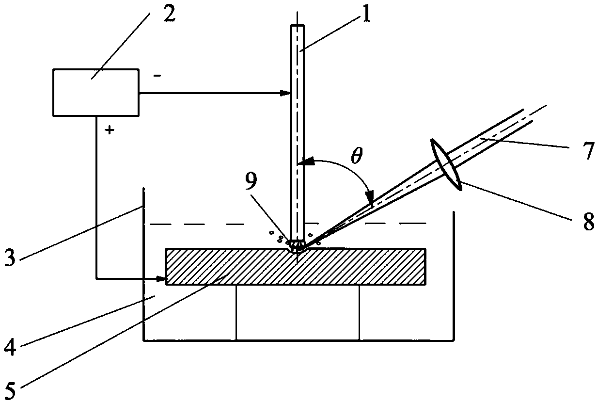
[0044] In this embodiment, the laser-induced discharge surface microstructure processing device such as figure 1 As shown, the working tank 3 contains a liquid working medium 4 , and the workpiece 5 is immersed in the working medium 4 . The microscale tool electrode 1 is connected to the negative pole of the power supply 2 , and the workpiece 5 is connected to the anode of the power supply 2 . A certain gap is maintained between the end surface of one end of the microscale tool electrode 1 and the surface of the workpiece 5 to be processed, the gap is in the range of 0.01 mm to 1.0 mm, and the gap is filled with the working medium 4 .

[0045] The laser light 7 generated by the laser converges in the gap through the focusing lens 8 .

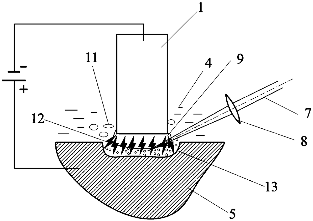
[0046] Such as figure 2 As shown, in the working state, the working medium in the gap boils and gasifies under the action of laser energy to generate a large number of bubbles 11, and the bubbles gather at the one end region of the microscal...

Embodiment 2

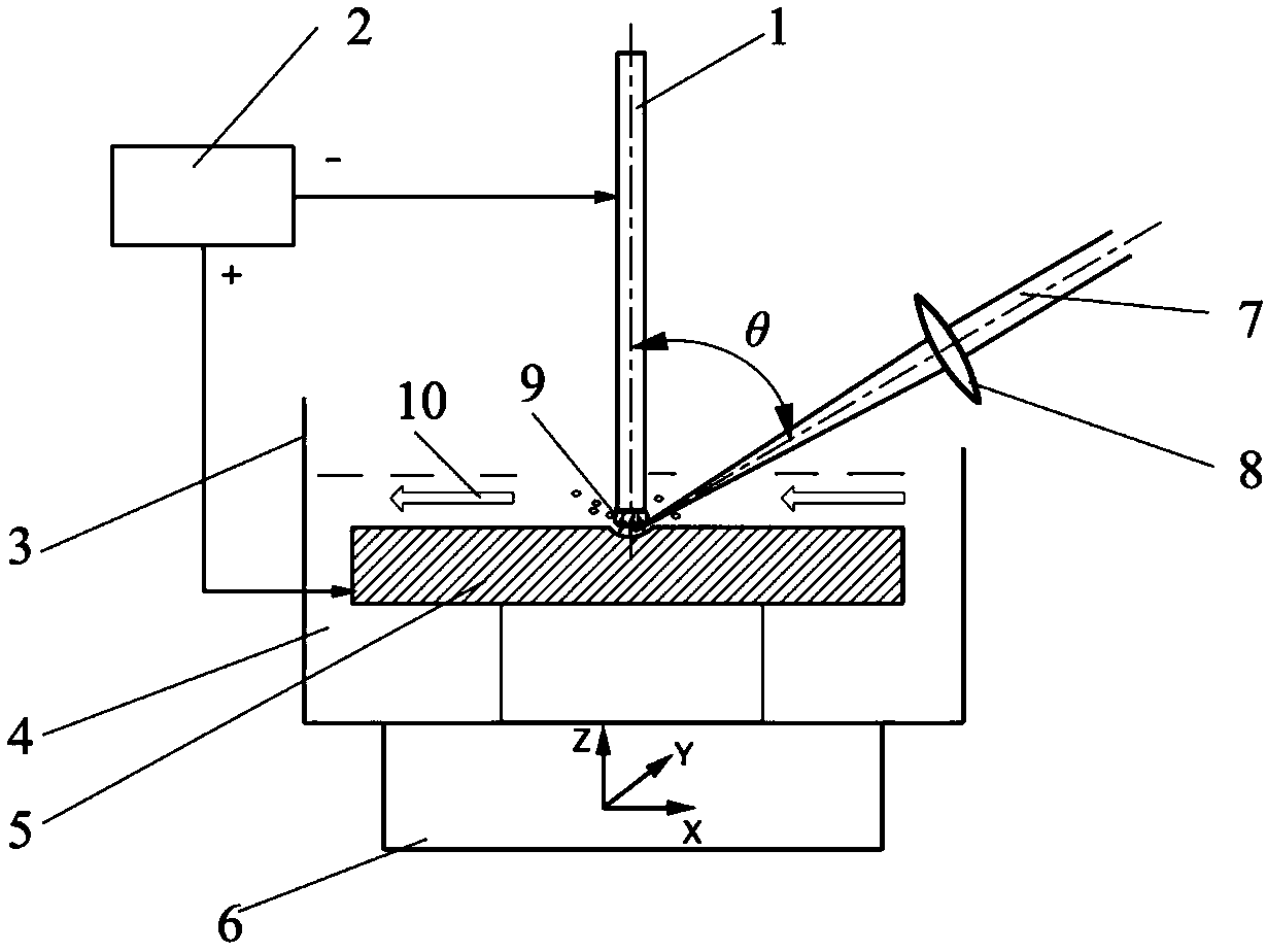
[0049] In this embodiment, the laser-induced discharge surface microstructure processing device such as image 3 As shown, the working tank 3 contains a liquid working medium 4 , and the workpiece 5 is immersed in the working medium 4 . The microscale tool electrode 1 is connected to the negative pole of the power supply 2 , and the workpiece 5 is connected to the anode of the power supply 2 . The working tank 3 is installed on the three-dimensional motion platform 6, and the three-dimensional motion platform 6 moves to drive the workpiece 5 to move. The end surface of one end of the micro-scale tool electrode 1 and the surface of the workpiece 5 to be processed maintain a certain gap, the distance of which is 0.02 mm to 0.5 mm, the gap is filled with the working medium 4, and the working medium 4 flows along the flow direction 10, that is, Flow in from one side of the gap and flow out from the other.

[0050] The laser light 7 generated by the laser converges in the gap thro...

Embodiment 3

[0054] In this embodiment, the structure of the laser-induced discharge surface microstructure processing device is basically the same as that of the laser-induced discharge surface microstructure processing device in Embodiment 2, the difference is as follows Figure 4 As shown, in this embodiment, the anode of the power supply 2 is connected to the auxiliary anode 23, and the distance between the auxiliary anode 23 and the microscale tool electrode 1 is not greater than 1 mm.


PUM


Abstract

The invention discloses a method and a device for machining laser-induced discharge surface micro-structures. The method includes connecting micro-scale tool electrodes with negative electrodes of power sources, keeping certain gaps between the end surface of an end of each micro-scale tool electrode and the surfaces of to-be-machined regions of workpieces and filling the gaps with liquid work media; converging laser light in the gaps, gasifying the work media under the effect of energy of the laser light and generating continuous gas at the end of each micro-scale tool electrode; turning on the power sources, forming electric circuits between negative electrodes and positive electrodes, generating breakdown discharge when the strength of electric fields in the gaps is higher than the breakdown strength of the gas, and removing the surfaces of the to-be-machined regions of the workpieces by means of corrosion by high temperatures so as to machine fine structures on the surfaces of theworkpieces. The method and the device have the advantages that micro-structures of conductive materials or non-conductive materials can be machined by the aid of the method under corrosive electrolytesolution inapplicable conditions, the to-be-machined regions of the workpieces and the distances of the gaps can be regulated and controlled, and accordingly the micro-structures with different contours can be machined by the aid of the method and the device.

Description

technical field [0001] The present application relates to a microstructure compound processing method, and relates to a laser-induced discharge surface microstructure processing method and its device, which can be applied to the processing of the surface microstructure of conductive materials, non-conductive materials and semiconductor material workpieces. Background technique [0002] With the progress and development of science and technology, the trend of miniaturization of products and components is becoming more and more obvious, and various micro electromechanical systems (Micro Electro Mechanical System, MEMS) are more widely used in aerospace, automotive, microelectronics, precision navigation and other fields . As a result, there is an increasing demand for precise microfabrication techniques for microstructures. [0003] The current microfabrication technology is often only suitable for a certain type of specific materials or has certain limitations. For example,...

Claims


Application Information

Patent Timeline
IPC IPC(8): B23K26/00B23K26/352
CPCB23K26/352
Inventor 王玉峰张文武
Owner NINGBO INST OF MATERIALS TECH & ENG CHINESE ACADEMY OF SCI
Why Eureka
Try Eureka