Pixel structure and display panel

A pixel structure and pixel electrode technology, which is applied in the direction of instruments, nonlinear optics, optics, etc., can solve problems such as dark lines and affect the direction of the liquid crystal branch pretilt angle, so as to reduce the occurrence of dark lines, reduce poor alignment, and strengthen the side The effect of the electric field

Active Publication Date: 2021-07-27
TCL CHINA STAR OPTOELECTRONICS TECH CO LTD
View PDF7 Cites 0 Cited by
  • Summary
  • Abstract
  • Description
  • Claims
  • Application Information

AI Technical Summary

Problems solved by technology

[0007] However, the lateral electric field 603 of the pixel structure 60 is a very weak electric field, and the pretilt angle of the liquid crystal molecules 63 is not only formed under the slit 612, but also is affected by the topography produced by other film layers in the display panel, so as to Black spacer (Black Photo Spacer, BPS) technology as an example, on the gate (gate) line, due to the existence of BPS, a high topography is formed, which will seriously affect the pretilt angle direction of the liquid crystal branch, resulting in dark lines

Method used


Image

  • Pixel structure and display panel
  • Pixel structure and display panel
  • Pixel structure and display panel

Examples


Embodiment Construction

[0029] The following will clearly and completely describe the technical solutions in the embodiments of the present invention with reference to the accompanying drawings in the embodiments of the present invention. Obviously, the described embodiments are only some, not all, embodiments of the present invention. Based on the embodiments of the present invention, all other embodiments obtained by persons of ordinary skill in the art without creative efforts fall within the protection scope of the present invention.

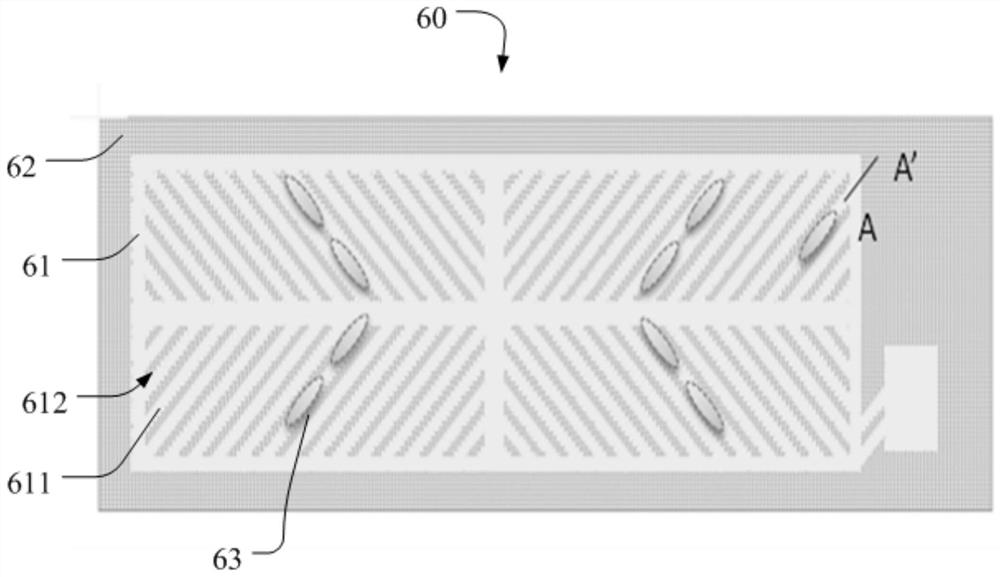
[0030] see Figure 5 , is a schematic diagram of the display panel 200 provided by the embodiment of the present invention. The display panel 200 includes a plurality of pixel structures 100 .

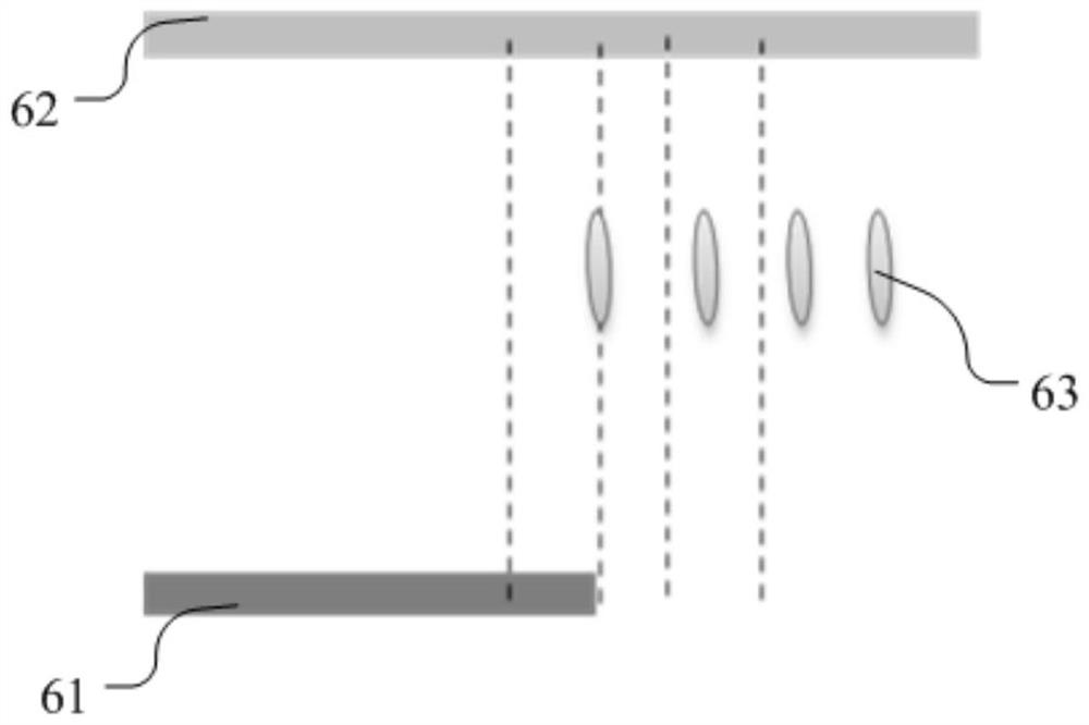
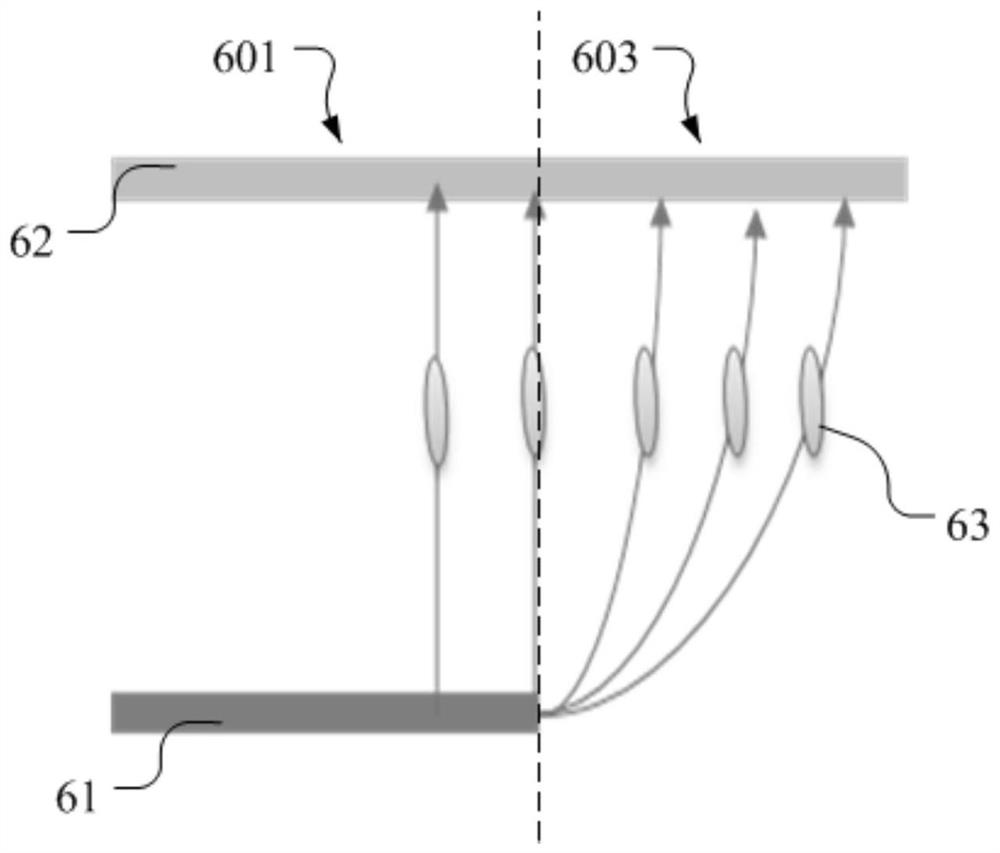
[0031] see Figure 6 , is a schematic diagram of the pixel structure 100 provided by the embodiment of the present invention. The pixel structure 100 includes a pixel electrode 10 and a common electrode 30 arranged in different layers. In this embodiment, the pixel elec...


PUM


Abstract

The present invention provides a pixel structure, including a pixel electrode and a common electrode arranged in different layers. The common electrode includes a main body and a peripheral portion wound around the main body. The main body is arranged opposite to the pixel electrode. A hollow area is formed adjacent to the peripheral portion. Since the main body and the peripheral part of the common electrode form a hollow area, when a voltage is applied to the common electrode and the pixel electrode, the lateral electric field can be strengthened, thereby reducing misalignment and dark lines. The invention also provides a display panel.

Description

technical field [0001] The present invention relates to the field of display technology, in particular to a pixel structure and a display panel. Background technique [0002] Active thin film transistor liquid crystal display (Thin Film Transistor-LCD, TFT-LCD) has been developed rapidly and widely used in recent years. Among them, the Vertical Alignment (VA) type TFT-LCD display panel has a very wide application in large-scale displays, such as televisions, due to its extremely high contrast ratio. [0003] HVA (High-Quality Vertical Alignment, high-quality vertical alignment technology) technology is currently the most used VA technology in large-size LCDs on the market. The HVA TFT-LCD display panel generally includes two upper and lower substrates, the upper substrate is a color filter substrate (CF substrate), the lower substrate is an array substrate (Array substrate), and the middle of the two substrates is a liquid crystal layer. [0004] Such as figure 1 As shown...

Claims


Application Information

Patent Timeline
Patent Type & Authority Patents(China)
IPC IPC(8): G02F1/1343
CPCG02F1/134309G02F1/134345
Inventor 叶岩溪
Owner TCL CHINA STAR OPTOELECTRONICS TECH CO LTD
Why Eureka
Try Eureka