Pixel circuit and liquid crystal display panel

A pixel circuit and pixel technology, applied in static indicators, nonlinear optics, instruments, etc., can solve problems such as large difference in channel aspect ratio, large IV characteristic fluctuation, large voltage jump, etc., to reduce horizontal crosstalk. Phenomenon, less crosstalk, less color cast effect

Inactive Publication Date: 2018-12-11
TCL CHINA STAR OPTOELECTRONICS TECH CO LTD
View PDF6 Cites 17 Cited by
  • Summary
  • Abstract
  • Description
  • Claims
  • Application Information

AI Technical Summary

Problems solved by technology

[0007] Affected by factors such as process stability, the channel aspect ratio of each thin film transistor in the above-mentioned 3T structure pixel circuit, especially the third thin film crystal T300, has a large difference, resulting in a relatively large fluctuation in its IV characteristic. Then the third thin film transistor T300 The impact of the discharge on the common electrode Acom on the array substrate side will be greater, resulting in a voltage jump of the common electrode Acom on the array substrate side when the screen is displayed, and the difference in voltage jump is large, which is affected by the voltage jump of the common electrode Acom on the array substrate side. Influenced by the screen display, there will be horizontal crosstalk (Crosstalk) phenomenon

Method used


Image

  • Pixel circuit and liquid crystal display panel
  • Pixel circuit and liquid crystal display panel
  • Pixel circuit and liquid crystal display panel

Examples


Embodiment Construction

[0038] In order to further illustrate the technical means adopted by the present invention and its effects, the following describes in detail in conjunction with preferred embodiments of the present invention and accompanying drawings.

[0039] The invention provides a pixel circuit.

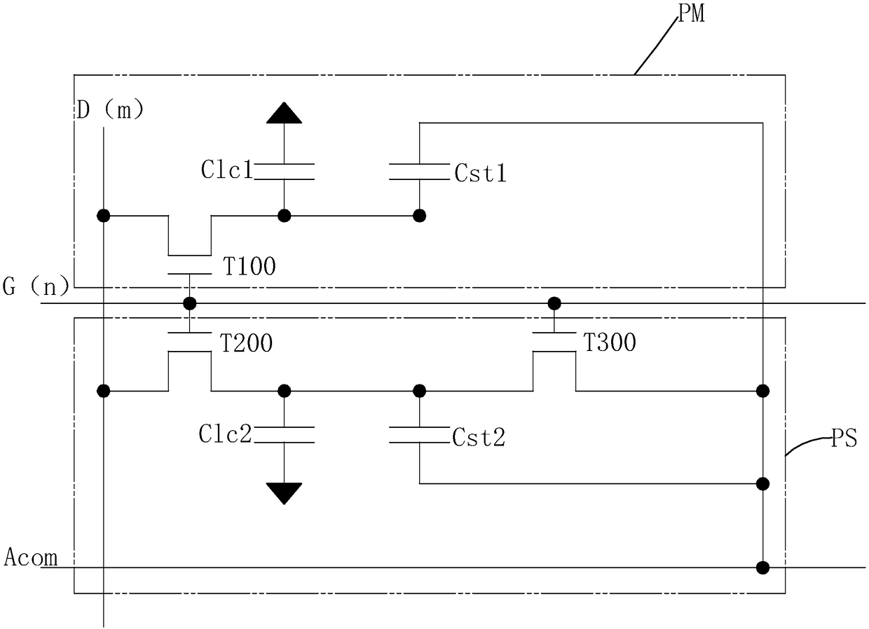
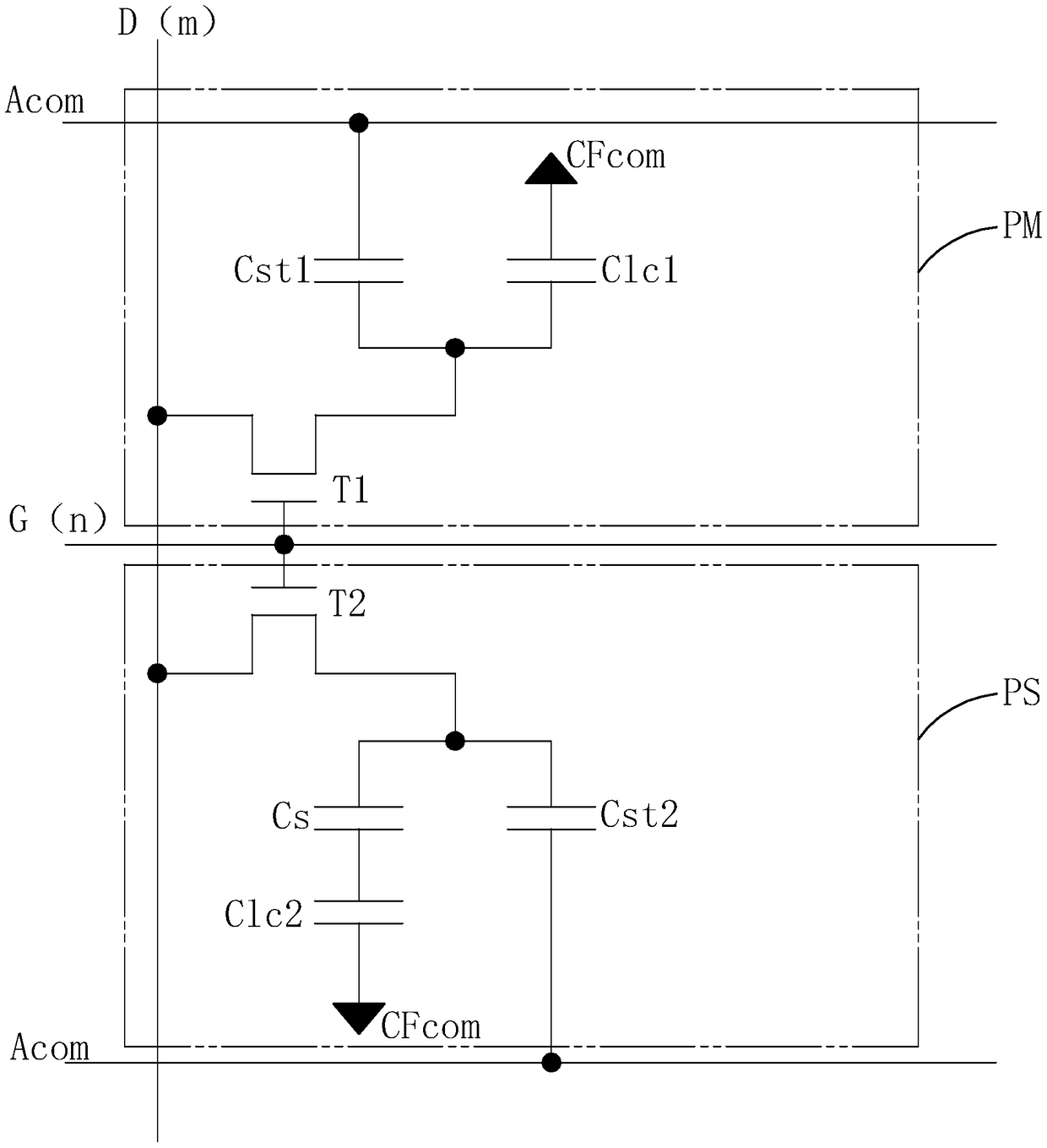
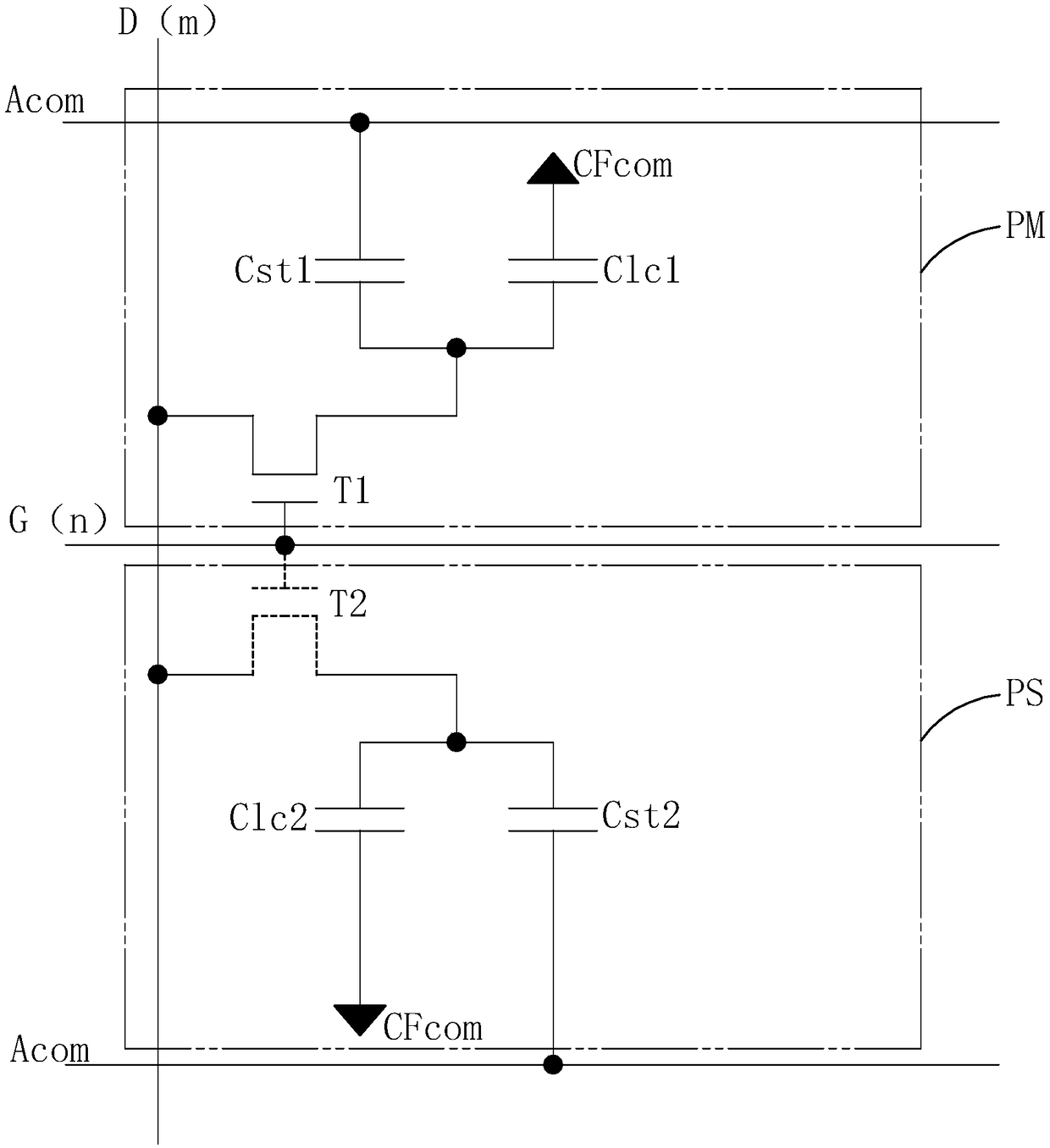
[0040] see figure 2 , the first embodiment of the pixel circuit of the present invention adopts 2T, that is, only two thin film transistor structures, including a pixel main area PM and a pixel sub area PS.

[0041] The main area PM of the pixel is provided with a main area thin film transistor T1 , a main area storage capacitor Cst1 and a main area liquid crystal capacitor Clc1 . The gate of the thin film transistor T1 in the main region is electrically connected to the scanning line G(n) (n is a positive integer, indicating the number of rows where the pixel is located), and the source is electrically connected to the data line D(m) (m is a positive integer, Indicates the number of columns ...


PUM


Abstract

The invention provides a pixel circuit and a liquid crystal display panel. The pixel circuit is in a 2T structure; on the one hand, a subarea liquid crystal capacitor (Clc2) is connected in series with a voltage-dividing capacitor (Cs), or the channel length-to-width ratio of a subarea thin-film transistor (T2) is smaller than that of a main-area thin-film transistor (T1), so that the voltage of the subarea liquid crystal capacitor (Clc2) is lower than that of a main-area liquid crystal capacitor (Clc1) to improve color shift significantly; on the other hand, compared with an existing pixel circuit in a 3T structure, the pixel circuit omits a third thin-film transistor which is used for discharging in a pixel subarea, thereby eliminating influence of discharging of the third thin-film transistor on common electrodes (Acom) of an array substrate, reducing horizontal crosstalk and further improving the pixel opening rate.

Description

technical field [0001] The invention relates to the technical field of liquid crystal display, in particular to a pixel circuit and a liquid crystal display panel. Background technique [0002] Liquid Crystal Display (LCD), referred to as LCD panel, has many advantages such as thin body, power saving, no radiation, etc., and has been widely used, such as: LCD TV, smart phone, digital camera, tablet computer, computer screens, or laptop screens, etc., dominate the field of flat panel displays. [0003] The liquid crystal display panel is composed of a color filter substrate (Color Filter, CF), a thin film transistor array substrate (ThinFilm Transistor Array Substrate, TFT Array Substrate), and a liquid crystal layer (Liquid Crystal Layer) disposed between the two substrates. A plurality of pixels (Pixels) arranged in an array are arranged in the liquid crystal display panel. When a driving voltage is applied to the two substrates, each pixel displays under the driving of th...

Claims


Application Information

Patent Timeline
Patent Type & Authority Applications(China)
IPC IPC(8): G02F1/1362G09G3/36
CPCG02F1/136213G02F1/13624G09G3/3648G02F2201/40G09G3/3607G09G2300/0426G09G2320/0242G02F1/1368G02F1/136222
Inventor 王金杰
Owner TCL CHINA STAR OPTOELECTRONICS TECH CO LTD
Why Eureka
Try Eureka