Lithography method

A lithography and developer technology, applied in photography, optics, opto-mechanical equipment, etc., which can solve the problems of photoresist film loss, increased line width roughness, pattern deformation, etc.

Inactive Publication Date: 2018-12-11
TAIWAN SEMICON MFG CO LTD
View PDF0 Cites 0 Cited by
  • Summary
  • Abstract
  • Description
  • Claims
  • Application Information

AI Technical Summary

Problems solved by technology

However, developing polyhydroxystyrene photoresists in existing negative tone developers is accompanied by various problems that cause photoresist film loss, increased line edge roughness, increased line width roughness, and pattern distortion

Method used


Image

  • Lithography method
  • Lithography method
  • Lithography method

Examples


Embodiment Construction

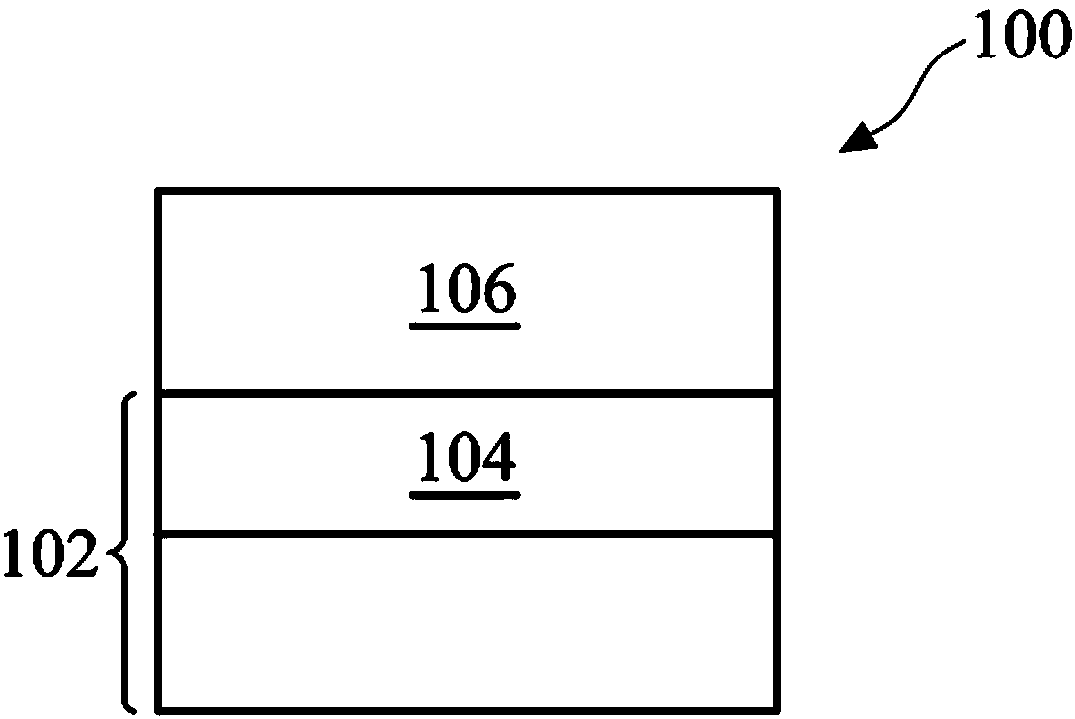
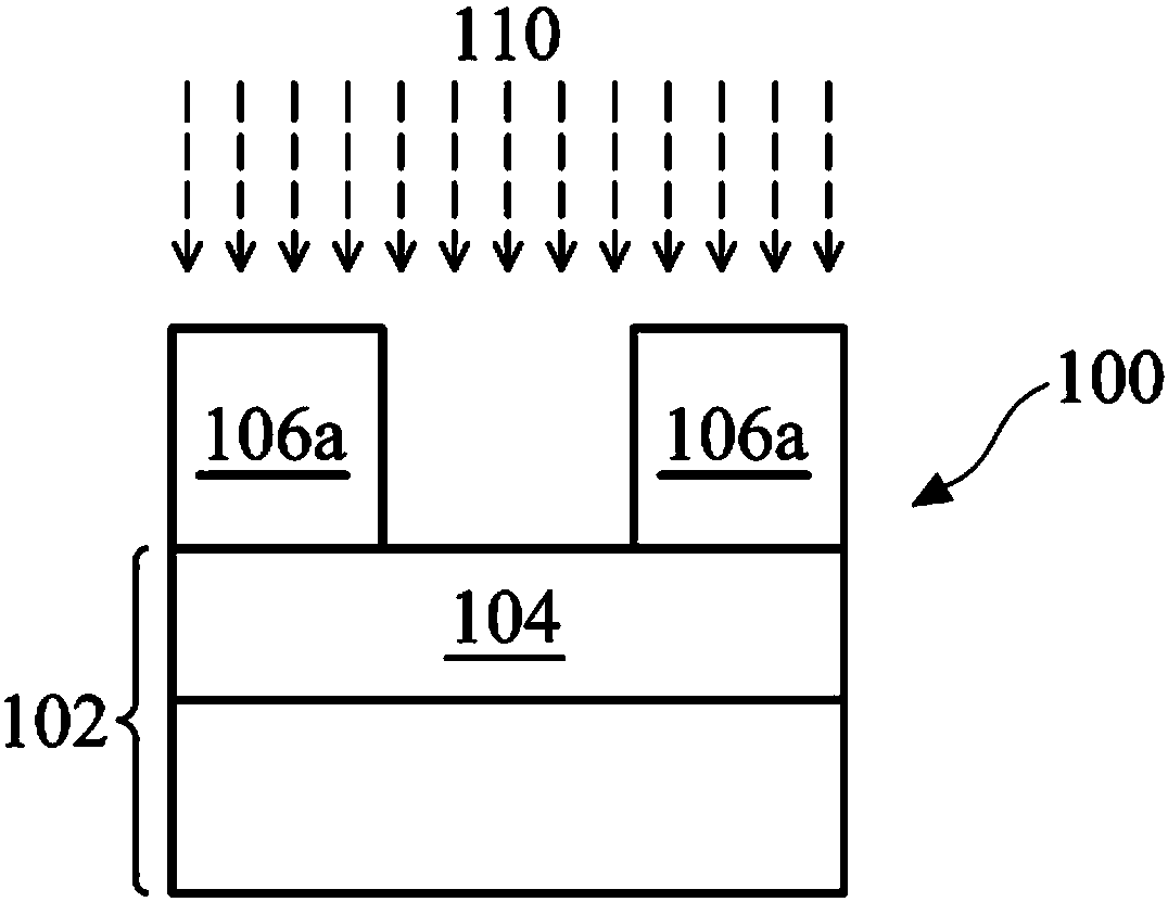
[0043] Different embodiments or examples provided below may implement different configurations of the present invention. The examples of specific components and arrangements are used to simplify the invention and not to limit the invention. For example, a statement that a first structure is formed on a second structure includes direct contact between the two, or there are other additional structures between the two instead of direct contact. In addition, numbers may be repeated in various examples of the present invention, but these repetitions are only for simplification and clarity of description, and do not mean that units with the same numbers in different embodiments and / or arrangements have the same corresponding relationship.

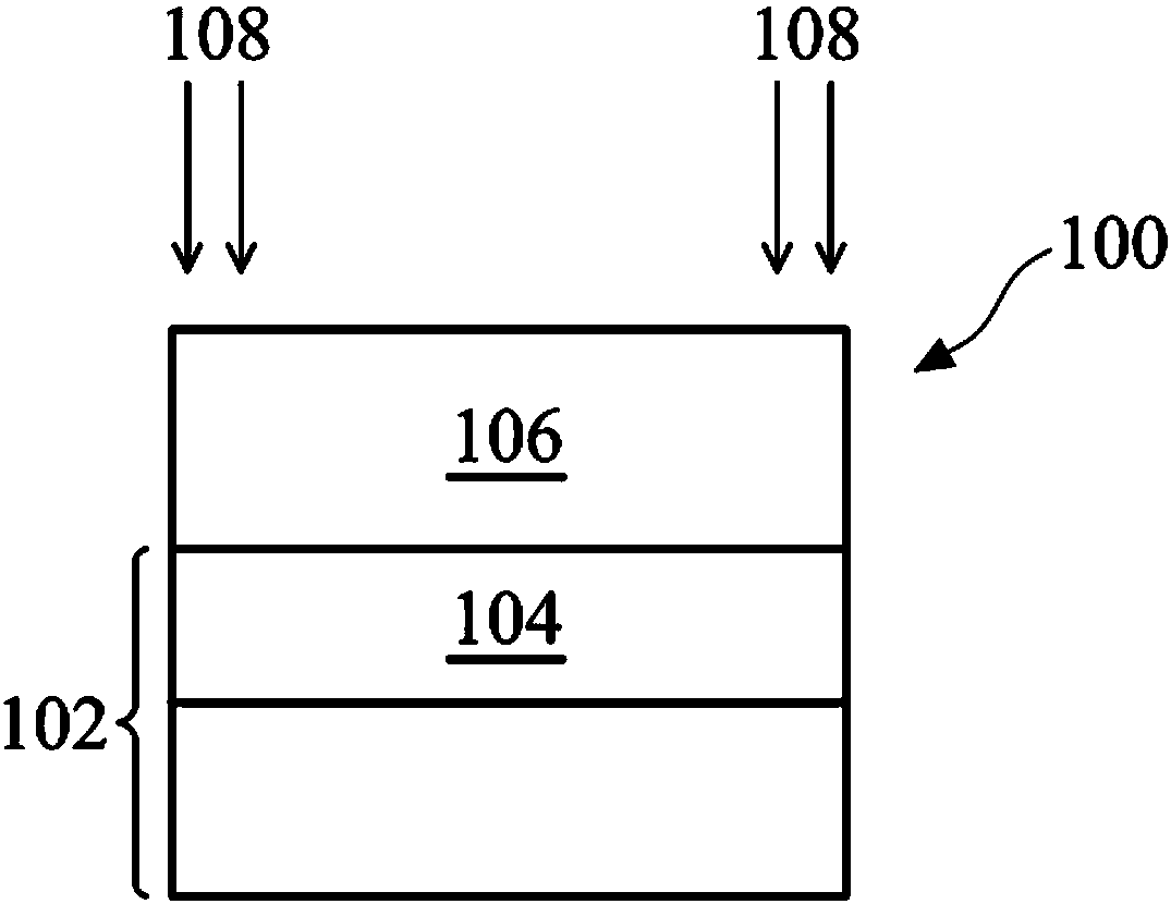
[0044] In addition, spatial relative terms such as "beneath", "beneath", "below", "above", "above", or similar terms may be used to simplify the relationship between one element and another element in the illustrations. relative relationship. S...


PUM

PropertyMeasurementUnit
wavelengthaaaaaaaaaa

Abstract

The present disclosure provides a method for lithography patterning. The method includes forming a resist layer over a substrate and performing an exposing process to the resist layer. The resist layer includes a polymer backbone, an acid labile group (ALG) bonded to the polymer backbone, a sensitizer bonded to the polymer backbone, a photo-acid generator (PAG), and a thermo-base generator (TBG).The method further includes baking the resist layer at a first temperature and subsequently at a second temperature. The second temperature is higher than the first temperature. The method further includes developing the resist layer in a developer, thereby forming a patterned resist layer.

Description

technical field [0001] Embodiments of the present invention relate to methods of fabricating semiconductor devices, and more particularly to compositions of photoresist films in EUV lithography and methods for using them. Background technique [0002] The semiconductor integrated circuit industry has experienced exponential growth. Technological advances in integrated circuit materials and design have resulted in each generation of integrated circuits being smaller and more complex than the previous generation. In the subject of integrated circuit evolution, functional density (the number of interconnected devices per unit chip area) usually increases as the geometric size (eg, the smallest component or circuit that can be formed by a process) shrinks. The advantage of shrinking the size of the process is to increase the production capacity and reduce the related costs, but it will also increase the complexity of the integrated circuit process. [0003] For example, EUV li...

Claims


Application Information

Patent Timeline
Patent Type & Authority Applications(China)
IPC IPC(8): G03F7/00
CPCG03F7/0035G03F7/0395G03F7/0397G03F7/325G03F7/38G03F7/0392G03F7/30G03F7/203
Inventor 刘朕与张雅晴吴承翰张庆裕林进祥
Owner TAIWAN SEMICON MFG CO LTD
Why Eureka
Try Eureka