Processing method for sector-shaped wafer
A processing method and wafer technology, applied in the fields of semiconductor/solid-state device parts, semiconductor/solid-state device testing/measurement, semiconductor devices, etc., can solve the problem of not being able to shorten the processing time, and achieve the effect of optimizing the processing feed
- Summary
- Abstract
- Description
- Claims
- Application Information
AI Technical Summary
Problems solved by technology
Method used
Image

Examples
Embodiment Construction
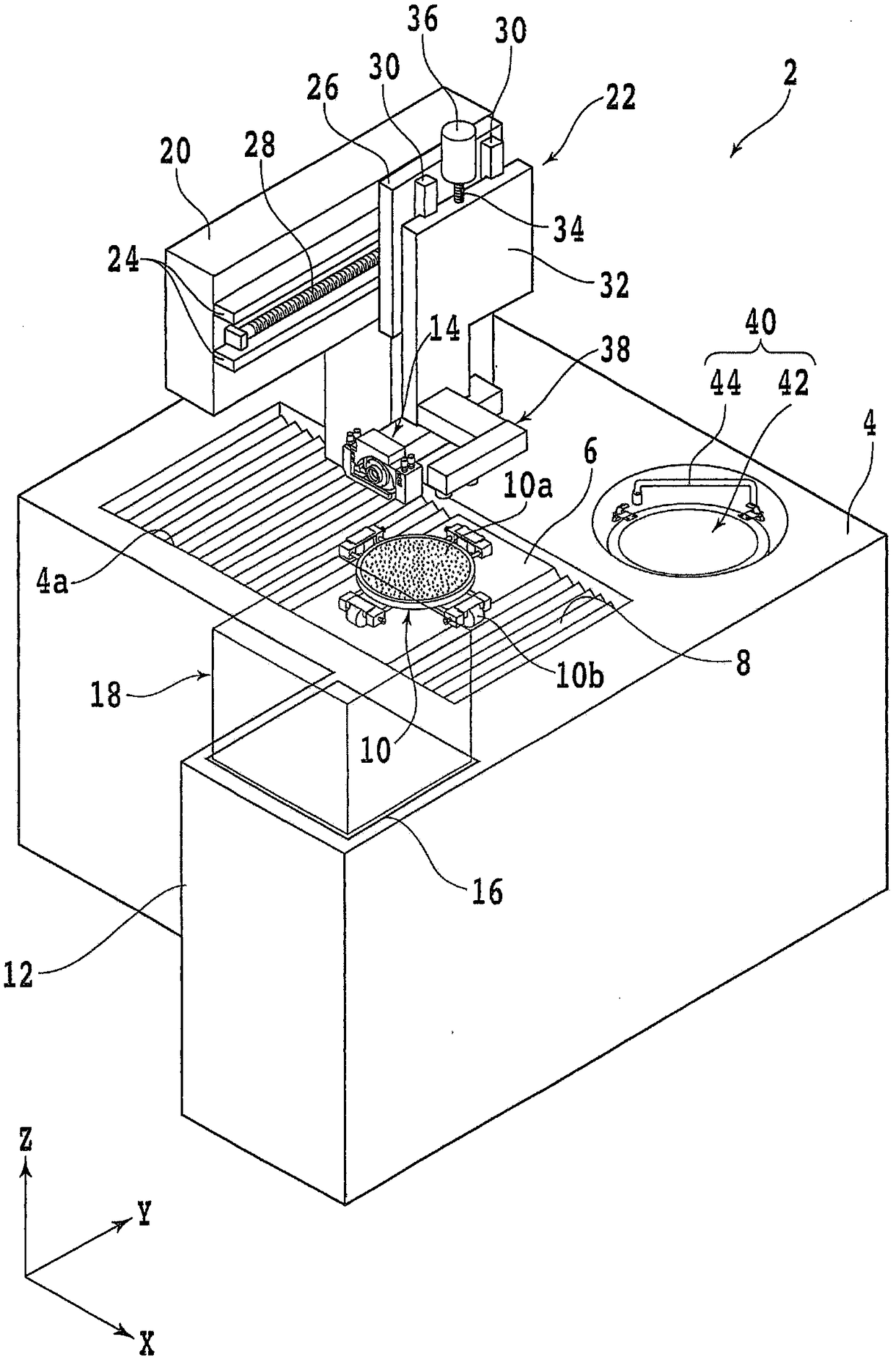
[0017] Hereinafter, embodiments of the present invention will be described in detail with reference to the drawings. refer to figure 1 , shows a perspective view of a cutting device according to an embodiment of the present invention. The cutting device 2 has a support base 4 , and a rectangular opening 4 a long in the X-axis direction (machining feed direction) is formed on the upper surface of the support base 4 .
[0018] An X-axis moving table 6, an X-axis moving mechanism (not shown) for moving the X-axis moving table 6 in the X-axis direction, and a dust-proof and drop-proof cover covering the X-axis moving mechanism are provided in the opening 4a. 8. This X-axis moving mechanism has a pair of X-axis guide rails (not shown) parallel to the X-axis direction, and the X-axis moving table 6 is slidably attached to the X-axis guide rails.
[0019] A nut portion (not shown) is provided on the lower surface side of the X-axis movable table 6, and an X-axis ball screw (not sh...
PUM
 Abstract
Description
Claims
Application Information
 - R&D
- Intellectual Property
- Life Sciences
- Materials
- Tech Scout
- Unparalleled Data Quality
- Higher Quality Content
- 60% Fewer Hallucinations
Browse by: Latest US Patents, China's latest patents, Technical Efficacy Thesaurus, Application Domain, Technology Topic, Popular Technical Reports.
© 2025 PatSnap. All rights reserved.Legal|Privacy policy|Modern Slavery Act Transparency Statement|Sitemap|About US| Contact US: help@patsnap.com