Double-gate thin-film transistor, preparation method of double-gate thin-film transistor, display panel and preparation method of display panel

A technology of thin-film transistors and substrates, which is applied in the direction of transistors, semiconductor/solid-state device manufacturing, and electric solid-state devices. It can solve problems such as threshold voltage bias and increase capacitor charging power consumption, and achieve the effect of reducing charging power consumption.

Active Publication Date: 2018-12-11
EVERDISPLAY OPTRONICS (SHANGHAI) CO LTD
View PDF16 Cites 11 Cited by
  • Summary
  • Abstract
  • Description
  • Claims
  • Application Information

AI Technical Summary

Problems solved by technology

[0004] In view of this, an embodiment of the present invention provides a double-gate thin film transistor and its manufacturing method, a display panel and its manufacturing method, to solve the problem of increasing the power consumption of capacitor charging due to the positive or negative threshold voltage in the existing OLED display technology. technical problem

Method used


Image

  • Double-gate thin-film transistor, preparation method of double-gate thin-film transistor, display panel and preparation method of display panel
  • Double-gate thin-film transistor, preparation method of double-gate thin-film transistor, display panel and preparation method of display panel
  • Double-gate thin-film transistor, preparation method of double-gate thin-film transistor, display panel and preparation method of display panel

Examples


Embodiment Construction

[0041] In order to make the purpose, technical solution and advantages of the present invention clearer, the technical solution of the present invention will be fully described below through specific implementation in combination with the drawings in the embodiments of the present invention. Apparently, the described embodiments are some embodiments of the present invention, rather than all embodiments. Based on the embodiments of the present invention, all other embodiments obtained by persons of ordinary skill in the art without making creative efforts, All fall within the protection scope of the present invention.

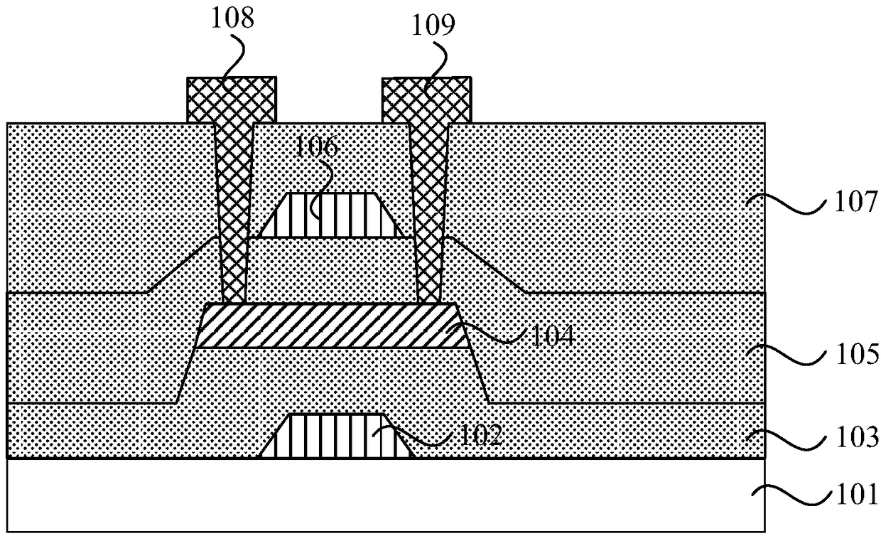
[0042] figure 2 is a schematic structural diagram of a dual-gate thin film transistor provided by an embodiment of the invention, please refer to figure 2 , the double-gate thin film transistor provided by the embodiment of the present invention may include:

[0043] Substrate 101;

[0044] a first gate electrode 102 located on the substrate 101;

[0045] ...


PUM


Abstract

The embodiment of the invention discloses a double-gate thin-film transistor, a preparation method of the double-gate thin-film transistor, a display panel and a preparation method of the display panel. The double-gate thin-film transistor comprises a substrate, a first gate electrode located on the substrate, a first gate insulating layer located on the first gate electrode, an active layer located on the first gate insulating layer, a second gate insulating layer located on the active layer, a second gate electrode located on the second gate insulating layer, an interlayer insulating layer located on the second gate electrode, and a source electrode and a drain electrode located on the interlayer insulating layer, wherein the source electrode and the drain electrode are electrically connected with the active layer through openings in the interlayer insulating layer and the second gate insulating layer. According to the technical scheme, a bias voltage signal is input to the first gate electrode, the threshold voltage of the thin-film transistor is adjusted, and the situation that the threshold voltage is deviated to be positive or negative is avoided.

Description

technical field [0001] Embodiments of the present invention relate to the technical field of semiconductors, and in particular to a double-gate thin film transistor and a manufacturing method thereof, a display panel and a manufacturing method thereof. Background technique [0002] Organic Light-Emitting Diode (OLED) has the advantages of small size, simple structure, self-illumination, high brightness, good image quality, large viewing angle, low power consumption and short response time, thus attracting widespread attention , It is very likely to become the next generation display technology to replace liquid crystal. [0003] In the prior art, two transistors T1 and T2 are usually used, and a 2T1C pixel drive circuit with a capacitor C is used to drive the OLED, such as figure 1 shown. However, because the threshold voltage of transistor T2 will drift with the working time, the threshold voltage of T2 will be negative or positive; and the threshold voltage of T2 may be ...

Claims


Application Information

Patent Timeline
Patent Type & Authority Applications(China)
IPC IPC(8): H01L29/786H01L21/336H01L21/34H01L27/32
CPCH01L29/6675H01L29/66969H01L29/78648H01L29/78654H01L29/78672H01L29/7869H10K59/1213H10K59/1201
Inventor 胡锐钦
Owner EVERDISPLAY OPTRONICS (SHANGHAI) CO LTD
Why Eureka
Try Eureka