A manufacturing method of PCB back drill hole

A production method and back-drilling technology, which are applied in printed circuit manufacturing, electrical components, printed circuits, etc., can solve the problem that the uniformity and fullness of back-drilling plug holes cannot be met, and the back-drilling air cannot be completely eliminated. Back-drilling holes or depressions to avoid hole blasting, avoid short circuits, and improve quality

Active Publication Date: 2018-12-11
ANHUI SUN CREATE ELECTRONICS
View PDF7 Cites 11 Cited by
  • Summary
  • Abstract
  • Description
  • Claims
  • Application Information

AI Technical Summary

Problems solved by technology

[0005] The traditional plug hole method can meet the plug hole requirements of ordinary back-drilled holes, but when the back-drilled hole is a back-drilled hole with a special structure, that is, the depth ratio of the back-drilled hole depth to the via hole depth is greater than or equal to 1, And when the back-drilling depth is greater than or equal to 0.5mm, the traditional plugging method is used to flow the resin ink from the back-drilling hole of the board into the via hole. Since the depth of the back-drilling hole is greater than or equal to the depth of the via hole, that is The volume of the back-drilled hole is large. When the via hole is filled, the back-drilled hole is not yet filled, which will make the air in the back-drilled hole unable to be completely removed. When the subsequent baking board is processed, the air will be heated and expanded, resulting in The resin in the back-drilled hole overflows, causing voids or depressions in the back-drilled hole. In the subsequent cap plating, the hole metallization solution enters the back-drilled hole, resulting in a short circuit in the back-drilled hole
Therefore, the traditional plug hole method cannot meet the uniformity and fullness requirements of the back-drilled plug hole with a special structure

Method used


Image

  • A manufacturing method of PCB back drill hole
  • A manufacturing method of PCB back drill hole
  • A manufacturing method of PCB back drill hole

Examples


Embodiment Construction

[0039] The following will clearly and completely describe the technical solutions in the embodiments of the present invention with reference to the accompanying drawings in the embodiments of the present invention. Obviously, the described embodiments are only some, not all, embodiments of the present invention. Based on the embodiments of the present invention, all other embodiments obtained by persons of ordinary skill in the art without making creative efforts belong to the protection scope of the present invention.

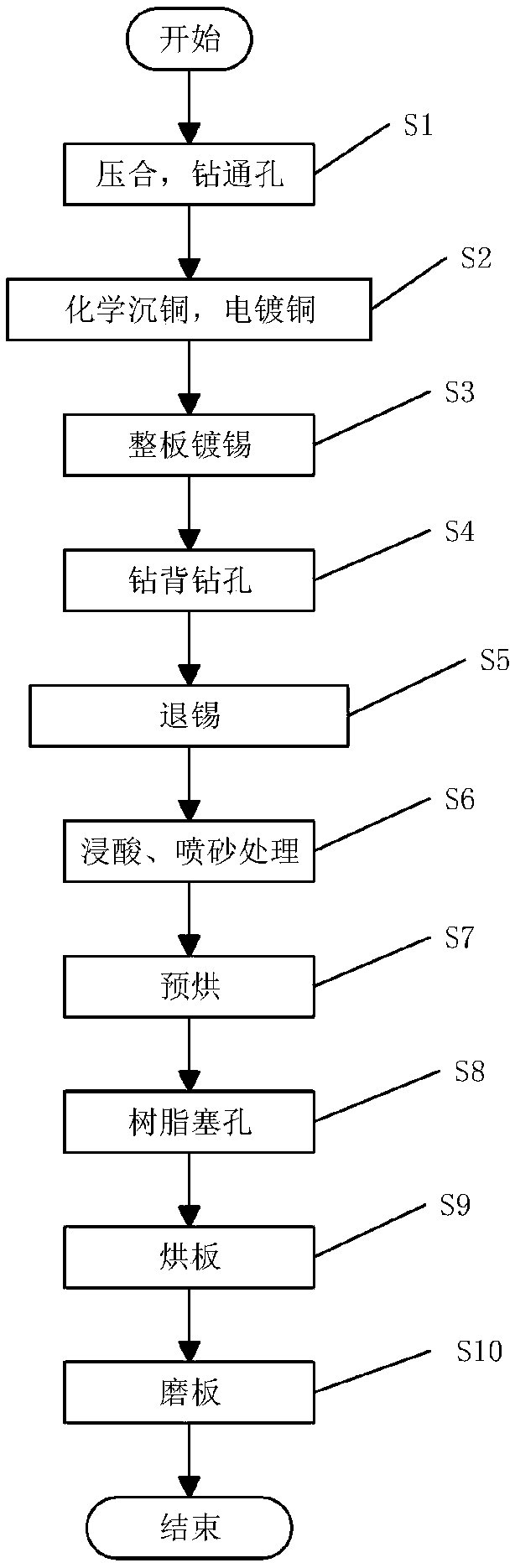
[0040] Such as figure 1 As shown, a method for manufacturing PCB back-drilled holes includes the following specific steps:

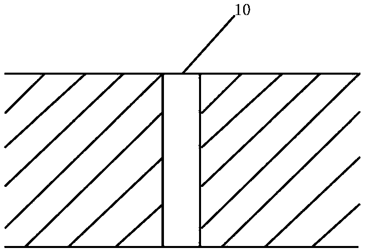
[0041] S1, the plates are pre-stacked and pressed together; if figure 2 As shown, the laminated plate is drilled once to obtain a through hole (10).

[0042] In step S1, the alignment of the plates is determined through the alignment system on the graph. In this implementation, the alignment is determined by placing concentric square...


PUM


Abstract

The invention discloses a manufacturing method of PCB back drill hole, which comprises the following steps: laminating, drilling through holes, chemical copper precipitation, electroplating copper, whole plate tin plating, drilling back drilling, tin removing, pre-drying plate, resin plug hole, drying plate and grinding plate; Wherein the back drill hole is a back drill hole having a special structure, wherein the depth ratio of the back drill hole depth to the through hole depth is greater than or equal to 1, and the depth of the back drill hole is greater than or equal to 0.5 mm; The pre-drying plate retains the residual temperature of the plate surface, and the residual temperature is higher than the ambient temperature for resin plug holes; The resin plug hole is plugged in such a waythat resin ink flows into the back hole from the through hole of the plate, and the whole back hole and the through hole are filled. The invention increases the plumpness of the plug hole of the backhole with the special structure, and improves the uniformity and reliability of the plug hole of the back hole with the special structure.

Description

technical field [0001] The invention relates to the technical field of multilayer microstrip board production, in particular to a method for manufacturing PCB back-drilled holes and resin plugging holes. Background technique [0002] In the PCB manufacturing process, through holes are needed to realize the connection between the inner layers. The through holes are usually formed by drilling machines, which require high processing accuracy. After drilling through holes, they need to undergo copper sinking, electroplating, etc. , forming a conductive layer in the through hole, so as to realize the connection between the inner layer lines, but the plated through holes of some PCB boards only need partial conduction, and the through holes after sinking copper and electroplating are all conduction Yes, this will cause the problem of connection at the end of the through hole, which will lead to the return of the signal, resulting in reflection, scattering, delay and other phenomen...

Claims


Application Information

Patent Timeline
Patent Type & Authority Applications(China)
IPC IPC(8): H05K3/00
CPCH05K3/0047H05K3/0094H05K2203/0214
Inventor 彭腾陈彦青管美章崔良端朱忠翰朱正大沈岳峰范晓春戴银海牛顺义
Owner ANHUI SUN CREATE ELECTRONICS
Why Eureka
Try Eureka