

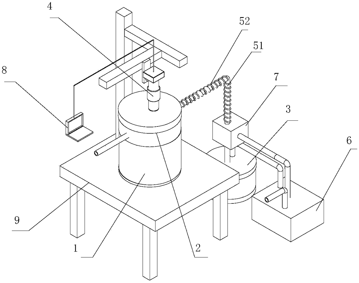
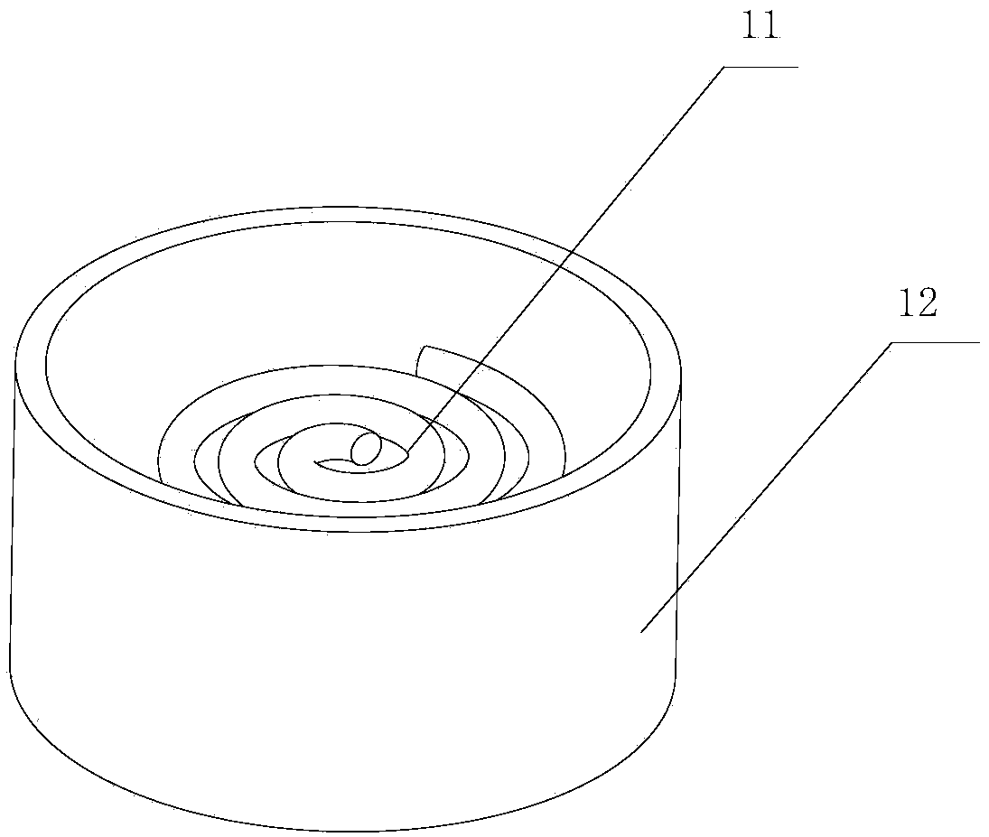
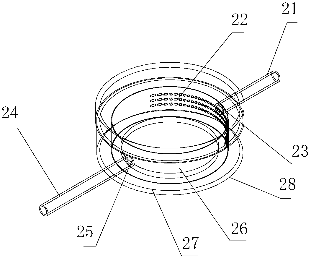
A semiconductor wet oxidation apparatus
A wet oxidation and semiconductor technology, used in semiconductor devices, semiconductor/solid-state device manufacturing, electrical components, etc., can solve problems such as affecting device performance, appearing dust particles, contaminating semiconductor wafer materials, etc., to achieve uniform temperature and good thermal conductivity. the effect of avoiding contamination of the sample
- Summary
- Abstract
- Description
- Claims
- Application Information
AI Technical Summary
Problems solved by technology
Method used
Image

Examples
Embodiment Construction
[0031] The following will clearly and completely describe the technical solutions in the embodiments of the application with reference to the accompanying drawings in the embodiments of the application. Apparently, the described embodiments are only part of the embodiments of the application, not all of them. Based on the implementation manners in this application, all other implementation manners obtained by persons of ordinary skill in the art without creative efforts fall within the scope of protection of this application.
[0032] It should be noted that when an element is referred to as being “disposed on” another element, it may be directly on the other element or there may also be an intervening element. When an element is referred to as being "connected to" another element, it can be directly connected to the other element or intervening elements may also be present.
[0033] Unless otherwise defined, all technical and scientific terms used herein have the same meaning...
PUM
 Abstract
Description
Claims
Application Information