A flexible display panel and a preparation method thereof

A flexible display and panel technology, used in semiconductor/solid-state device manufacturing, instruments, electrical components, etc., can solve the problems of internal stress concentration, small roughness, packaging failure, etc., and achieve the effect of reducing internal stress and small resistance

Active Publication Date: 2018-12-14
EVERDISPLAY OPTRONICS (SHANGHAI) CO LTD
View PDF9 Cites 12 Cited by
  • Summary
  • Abstract
  • Description
  • Claims
  • Application Information

AI Technical Summary

Problems solved by technology

At present, flexible OLED packaging films mainly adopt single-layer packaging and composite film packaging, but these technologies have disadvantages, that is, the surface of the film layer

Method used


Image

  • A flexible display panel and a preparation method thereof
  • A flexible display panel and a preparation method thereof
  • A flexible display panel and a preparation method thereof

Examples


Embodiment 1

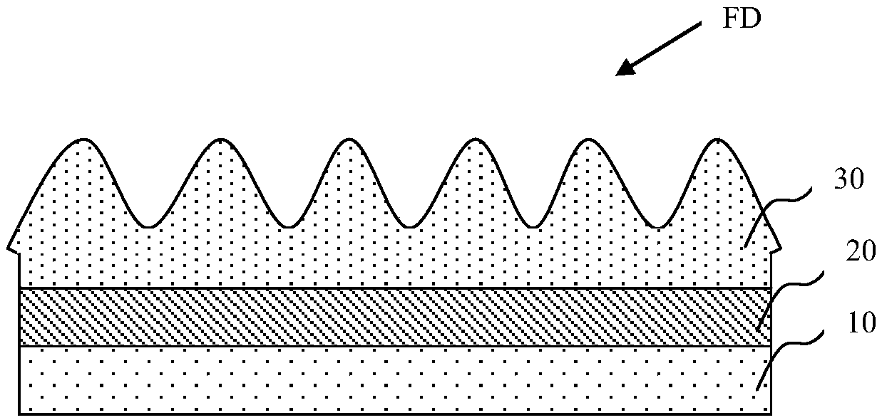
[0049] The surface of the packaging film used to package OLED flexible display panels is relatively flat and has small roughness. In the flexible process that requires repeated bending, the internal stress is often unable to be released smoothly, resulting in stress concentration inside, resulting in damage to the packaging film. Damaged encapsulation films cannot block external moisture and oxygen from entering the OLED device, and black spots may be formed on the display due to encapsulation failure.

[0050] Such as figure 1 As shown, this embodiment discloses a flexible display panel, which is characterized in that it includes:

[0051] Substrate 10;

[0052] An organic light emitting diode device array 20, covering the upper surface of the substrate 10;

[0053] The packaging film 30 covers the upper surface of the organic light emitting diode device array 20, and is used to package the organic light emitting diode device array 20 on the upper surface of the substrate 1...

Embodiment 2

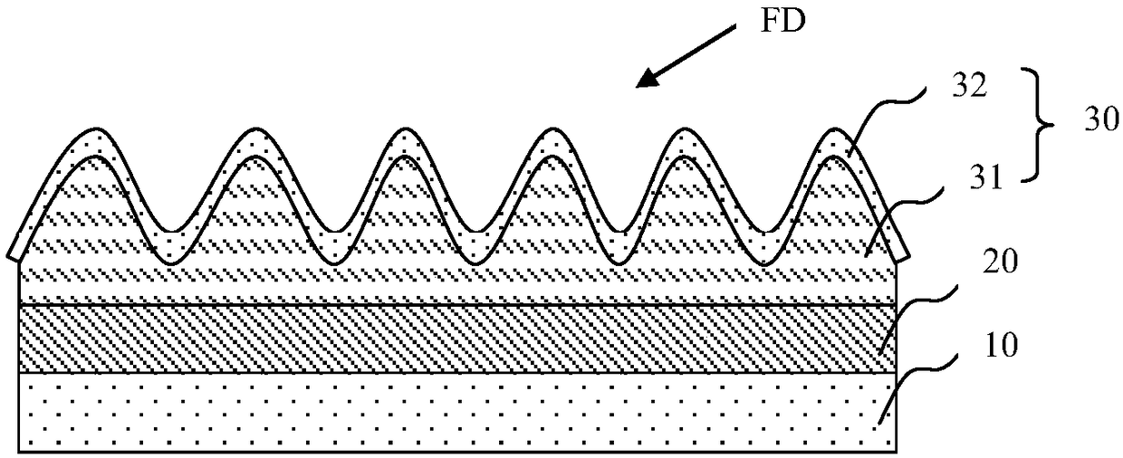
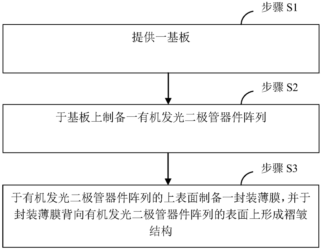
[0069] Such as image 3 As shown, it also includes a method for preparing a flexible display panel, and the formed structure can be as follows Figure 4 ~ Figure 5 As shown, can include:

[0070] Step S1, providing a substrate 10;

[0071] Step S2, preparing an organic light emitting diode device array 20 on the substrate;

[0072] Step S3 , preparing an encapsulation film 30 on the upper surface of the OLED device array 20 , and forming a wrinkle structure FD on the surface of the encapsulation film 30 facing away from the OLED device array 20 .

[0073] In the above technical solution, during the bending process of the flexible display screen, the wrinkled structure FD is formed on the surface of the packaging film 30 facing away from the organic light emitting diode device array 20, and the formed wrinkled structure FD receives little resistance, so that the packaging film 30 is formed The stress on the surface of the wrinkled structure FD can be released, so that the pa...


PUM

PropertyMeasurementUnit
Widthaaaaaaaaaa
Thicknessaaaaaaaaaa
Thicknessaaaaaaaaaa

Abstract

The invention discloses a flexible display panel and a preparation method thereof. The flexible display panel includes an organic light emitting diode device array covering the upper surface of the substrate; A packaging film covering the upper surface of the organic light emitting diode device array and used for packaging the organic light emitting diode device array on the upper surface of the substrate, and the packaging film is formed with a wrinkled structure opposite to the surface of the organic light emitting diode device array; The technical scheme has the beneficial effect that the wrinkled structure formed on the upper surface of the packaging film is utilized to reduce the internal stress in the bending process of the flexible screen so as to ensure that the packaging film after bending can still be kept intact.

Description

technical field [0001] The invention relates to the technical field of flat panel display devices, in particular to a flexible display panel and a preparation method thereof. Background technique [0002] With the continuous improvement of people's quality of life, various mobile terminals have become people's favorite devices, especially mobile terminal products with large screens and high-resolution displays are especially popular, because users have more and more requirements for display screens High, more new technologies have been invested in mobile terminal displays, such as OLED (Organic Light-Emitting Diode, organic light-emitting diode) display technology, due to its self-illumination, wide viewing angle, almost infinitely high contrast, low power consumption, The advantages of extremely high response speed and easy realization of flexible display have gradually become the mainstream of mobile terminal display screens. [0003] OLED display panels are often prepare...

Claims


Application Information

Patent Timeline
IPC IPC(8): H01L51/52H01L51/56H01L27/32G09F9/30
CPCG09F9/301H10K59/00H10K50/84H10K71/00
Inventor 欧阳攀
Owner EVERDISPLAY OPTRONICS (SHANGHAI) CO LTD
Why Eureka
Try Eureka