A novel fabrication method of interconnected silicon through hole with adjustable resistance

A manufacturing method and technology for interconnecting silicon, applied in separation methods, chemical instruments and methods, components of TV systems, etc., can solve problems such as heavy weight, large volume, and difficulty in integration, avoiding the need for process equipment and reducing resistance The effect of matching difficulty and avoiding stress concentration problems

Active Publication Date: 2018-12-18
BEIJING MXTRONICS CORP +1
View PDF9 Cites 0 Cited by
  • Summary
  • Abstract
  • Description
  • Claims
  • Application Information

AI Technical Summary

Problems solved by technology

[0003] The existing technology focuses on not adding the on-resistance of the TSV to the TSV, which requires an additional matching resistance, which has the disadvantages of large volume, heavy weight, and difficulty in integration.

Method used


Image

  • A novel fabrication method of interconnected silicon through hole with adjustable resistance
  • A novel fabrication method of interconnected silicon through hole with adjustable resistance
  • A novel fabrication method of interconnected silicon through hole with adjustable resistance

Examples


Embodiment Construction

[0036] Below in conjunction with accompanying drawing and specific embodiment the present invention is described in further detail:

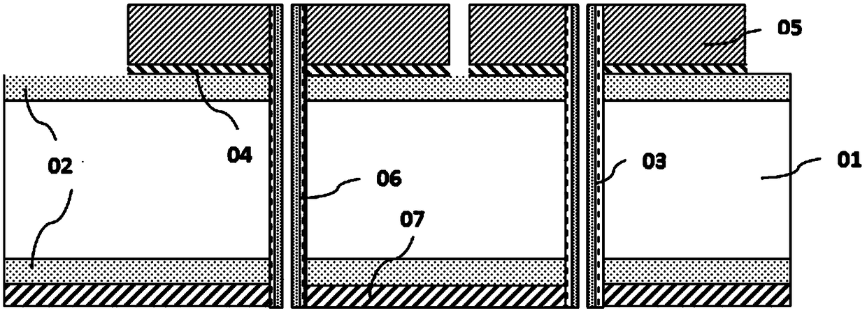
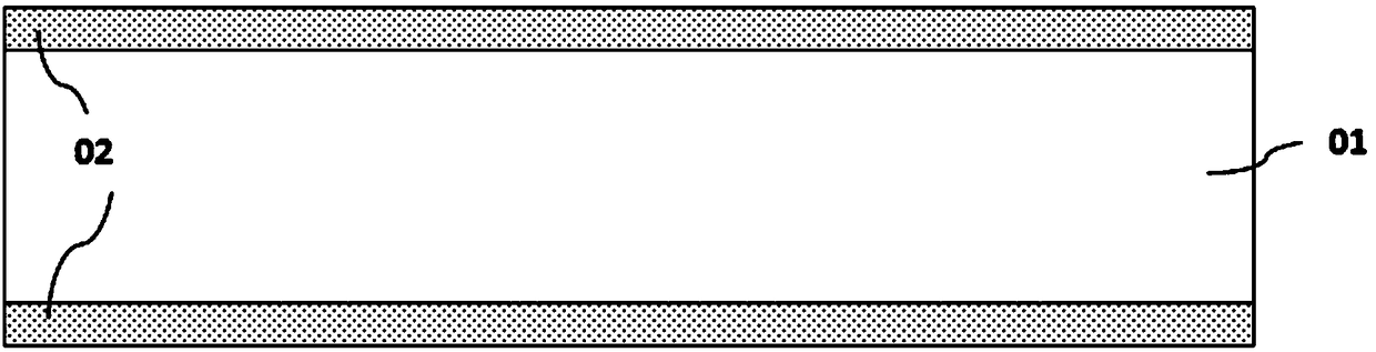
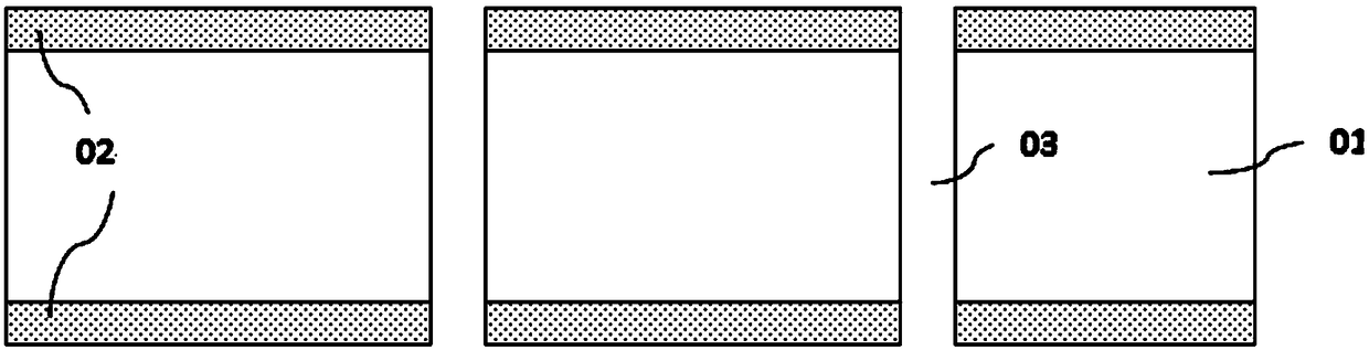
[0037] The invention relates to a new manufacturing method of interconnected through-silicon vias with adjustable resistance, which uses a silicon substrate to realize the manufacture of through-hole interconnections, and uses an electroplating process to control the resistance value of the through-hole resistance; figure 1 Shown is a side view of TSV interconnection. It can be seen from the figure that the interconnection of TSV is realized by using MEMS technology, including deep silicon etching process, metal film deposition process, thick resist photolithography process, and thick metal layer electroplating process. This via has significant resistive properties that can be used to compensate for the resistive properties of the devices it interconnects.

[0038] A novel manufacturing method of interconnected through-silicon vias with adjustab...


PUM

PropertyMeasurementUnit
Resistivityaaaaaaaaaa
Thicknessaaaaaaaaaa
Diameteraaaaaaaaaa

Abstract

The invention relates to a novel manufacturing method of an interconnected silicon through hole with adjustable resistance, which relates to the field of the manufacturing method of the interconnectedsilicon through hole, comprising the following steps: (1) oxidizing the upper bottom surface and the lower bottom surface of the high-resistance silicon; 2, etch that silicon through hole on the electric isolation layer; 3, depositing a metal film on that upper surface of the electrical isolation layer on the upper surface of the high-resistance silicon; 4, spreading photoresist on the upper surface of the seed lay of the metal film; 5, manufacturing an input / output terminal of an interconnected silicon through hole signal; 6, manufacturing to form a stratum interconnect layer; Step 7, electroplating the inner wall of the silicon through hole; 8, scribing the high-resistance silicon along a preset scribing path to separate the interconnected silicon through hole chips. The invention has simple process, can meet the compensation requirement of Wheatstone bridge arm resistance, reduces the matching difficulty of resistors, and realizes better process integration.

Description

technical field [0001] The invention relates to the field of a method for manufacturing interconnected through-silicon holes, in particular to a novel method for manufacturing interconnected through-silicon holes with adjustable resistance. Background technique [0002] Based on MEMS technology, new signal interconnection methods can be developed in the field of silicon technology packaging. This method can be used not only in the field of microelectronics, but also in fields such as mechanics, acoustics, fluids, optoelectronics, and biomedicine. Such new applications (including sensors and actuators, etc.) are often developed on separate chips due to rapidly growing market demands for pressure sensors, accelerometers and gyroscopes, projected micromirrors, inkjet print heads, etc. Emerging markets that are being formed (including wireless communications, medical care, hygiene, and wearable markets) and so on. These new products are characterized by first using silicon dee...

Claims


Application Information

Patent Timeline
IPC IPC(8): B81B7/02B81B1/00B81C1/00
CPCB81B1/00B81B7/02B81C1/00095
Inventor 屈怀泊刘燕谢强孙金池
Owner BEIJING MXTRONICS CORP
Why Eureka
Try Eureka