Electronic speckle pattern interference detection system and lossless detection method for failures of solder balls

A technology of electronic speckle interference and detection method, applied in the field of electronic speckle interference system, can solve the problems of low detection efficiency, poor process integration and high cost, and achieve the effects of good industrial integration, low cost and simple structure

Inactive Publication Date: 2011-08-03
FUDAN UNIV
View PDF1 Cites 11 Cited by
  • Summary
  • Abstract
  • Description
  • Claims
  • Application Information

AI Technical Summary

Problems solved by technology

This method has many steps, high cost, poor pr

Method used


Image

  • Electronic speckle pattern interference detection system and lossless detection method for failures of solder balls
  • Electronic speckle pattern interference detection system and lossless detection method for failures of solder balls
  • Electronic speckle pattern interference detection system and lossless detection method for failures of solder balls

Examples


Embodiment 1

[0044] Example 1 Electronic speckle interference test system for detecting solder ball failure in board-level assembly ball grid array package

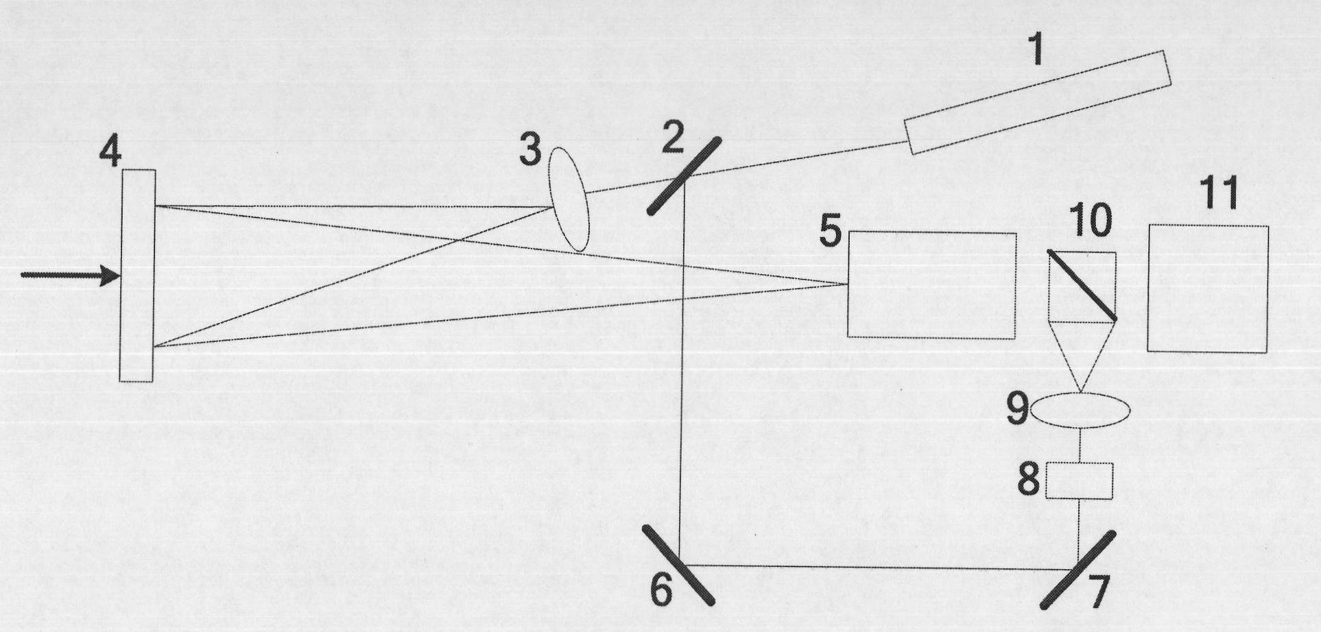
[0045] The system includes: fixing and loading parts, off-plane displacement test optical path part of electronic speckle interference and computer data processing part. Among them, the fixing and loading part is used to provide stable clamping and mechanical loading for the tested board-level assembly ball grid array package device; the off-plane displacement test optical path part is used to form interference fringes after the package is deformed under mechanical load, that is, the surface micro Displacement: The computer data processing part is used to collect fringes, perform phase unpacking and displacement calculation, locate the failure area, and through further calculation and processing, finally determine the failure solder joint and its damage degree.

[0046] Reference figure 1 Describes the optical path part of the off-plane di...

Embodiment 2

[0049] Example 2 Electronic speckle interference test method for solder ball failure in ball grid array package

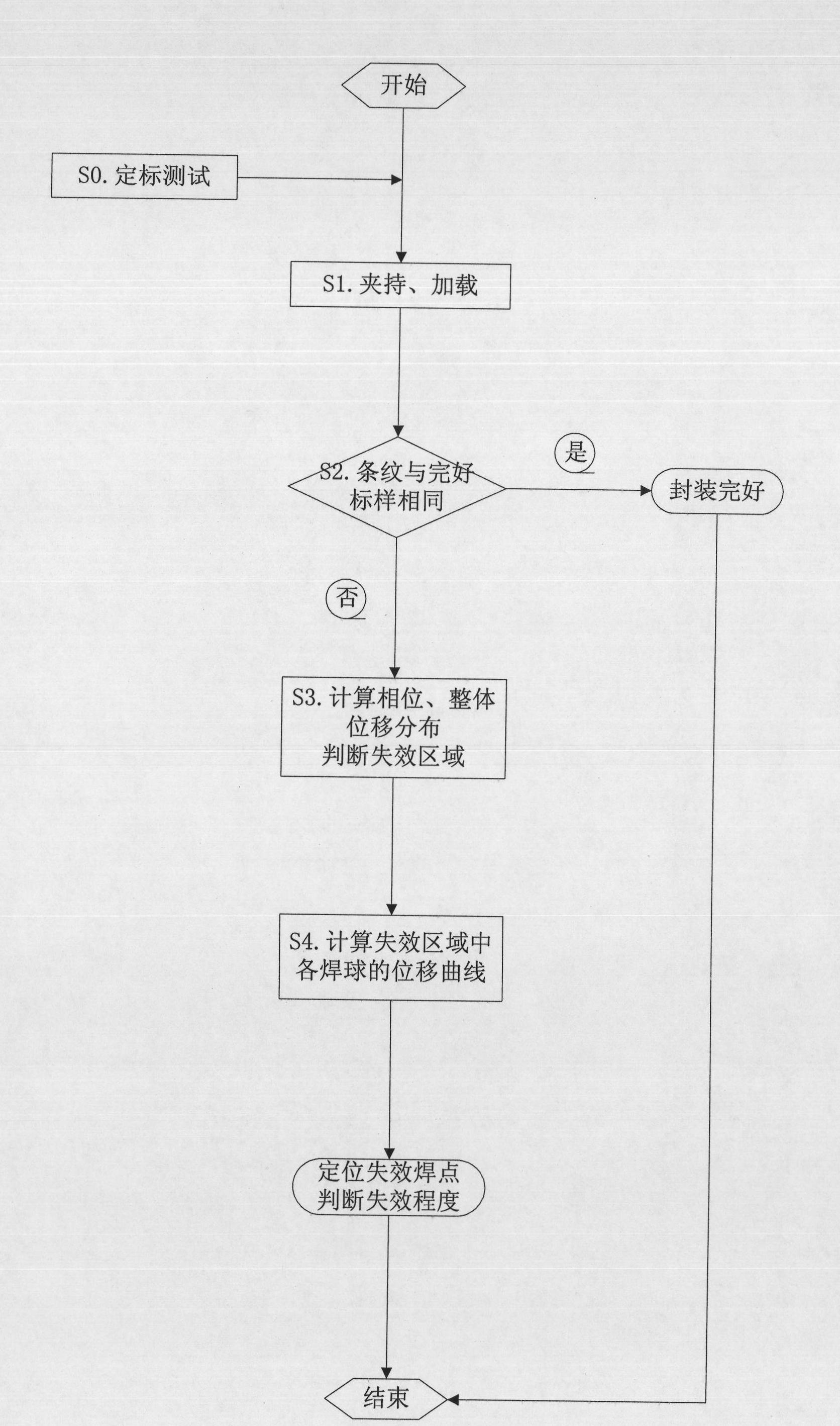
[0050] Reference image 3 Describes the electronic speckle interference test method for detecting the failure of solder balls in the ball grid array package corresponding to the embodiment of the present invention. image 3 It is the flow chart of the test method. First, in step S0, a calibration test is performed on a known intact ball grid array package of the same model. The packaged device is fixed by the fixing and loading part, and a mechanical load is applied to the back of the packaged device. The load should remain unchanged during the entire stripe extraction and phase shift process. At the same time, the fringe pattern is obtained by the off-plane displacement test optical path of the electronic speckle interference, and collected by the computer. The computer data processing part performs a series of calculations on the input information, including the ov...

Embodiment 3

[0056] Example 3 Sample detection

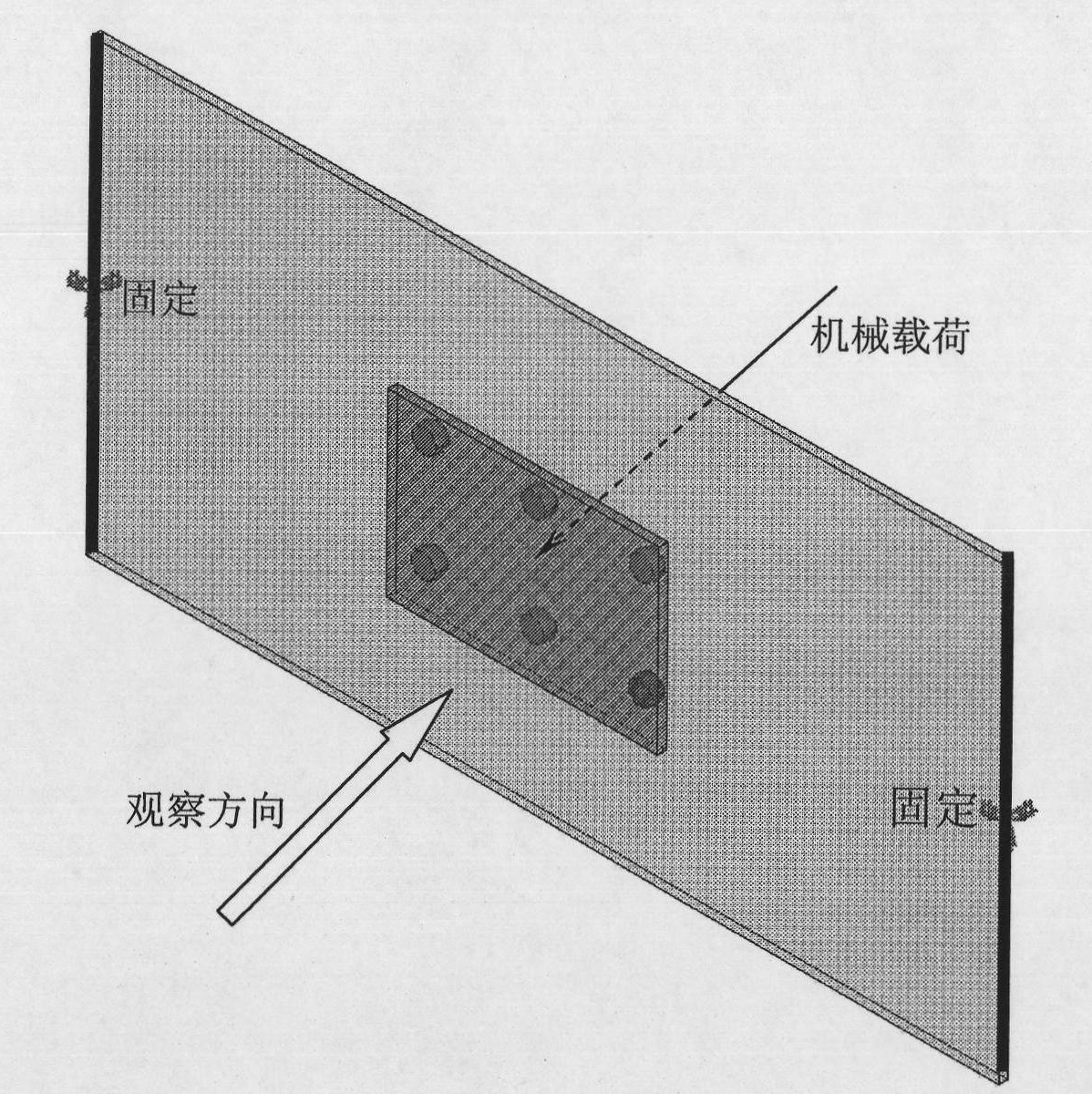
[0057] figure 2 It is a schematic diagram of the sample to be tested. The sample is a PCB board with a length, width and thickness of 14.60×10.68×0.92mm through electroplating, etching and other processes to generate basic interconnections such as pads and leads, and planting a 3×2 lead-tin solder ball array as an analog device. The diameter of the solder balls is 0.76mm, the lateral spacing is 4.00mm, and the longitudinal spacing is 6.00mm. Then the analog device is reflow soldered to a PCB board with length, width and thickness of 100, 40, and 0.92 mm. Samples under three conditions of intact formation, delamination of the solder ball on the lower right corner of the device, and drop off of the solder ball on the lower right corner of the device.

[0058] Figure 4-6 It is an out-of-plane displacement fringe diagram obtained by using the electronic speckle interference test system corresponding to the present invention to separately detect s...


PUM


Abstract

The invention belongs to the field of electronic packaging and relates to an electronic speckle pattern interference detection system and method for failures of solder balls in board assembly ball grid array packaging devices. The system provided by the invention comprises a detection sample fixing and loading part, an electronic speckle pattern interference out-of-plane displacement testing light path part and a computer data analyzing and processing part, wherein the electronic speckle pattern interference out-of-plane displacement testing light path part is used for forming the interference fringes of the detection sample after deforming under a mechanical load, namely out-of-plane micro-displacement information; the computer data analyzing and processing part is used for collecting the fringes, carrying out phase unpacking and displacement computation and positioning failure regions; and the out-of-plane displacement fringes of a standard sample and the sample are compared to determine whether the sample is subjected to the failure of the solder balls or not. The system provided by the invention has the advantages of simple composition components, no damage on the devices in a measuring course, simple and convenient detection method, good process integrity and real-time measurement realization on a production line, thereby greatly enhancing the detection efficiency of the failure of the solder balls in the board assembly ball grid array packaging devices.

Description

Technical field [0001] The invention belongs to the field of electronic packaging, and relates to an Electronic Speckle Pattern Interferometry (ESPI, Electronic Speckle Pattern Interferometry) system for detecting the failure of solder balls in a board-level assembled ball grid array (BGA, Ball GridArray) package device, and a detection method thereof. Background technique [0002] The ball grid array package is a surface mount form in which the I / O terminals are distributed in an array with spherical or cylindrical solder joints. It can realize the high I / O count, high performance, multi-function and high density of the package, and it has been widely used in the field of electronic packaging. However, during assembly processes such as reflow soldering, the ball grid array package may fail due to thermal mismatch or other stresses in individual solder joints such as cracks, delamination or even falling off. And the solder joints are not exposed after assembly, and the quality i...

Claims


Application Information

Patent Timeline
IPC IPC(8): G01N21/88
Inventor 高云霞王珺肖斐
Owner FUDAN UNIV
Why Eureka
Try Eureka