Reconfigurable TeraHertz wave super-diffraction focusing device based on voltage regulation and control

A voltage regulation and device technology, applied in the field of terahertz wave focusing, can solve problems such as difficult to meet requirements and small focal length, and achieve the effect of reducing crosstalk and enhancing reliability

Inactive Publication Date: 2018-12-18
CHONGQING UNIV
View PDF4 Cites 2 Cited by
  • Summary
  • Abstract
  • Description
  • Claims
  • Application Information

AI Technical Summary

Problems solved by technology

[0004] Although the existing terahertz wave technology has achieved super-resolution focusing, they are all based on the principle of near-field optics, and the focal length is extremely

Method used


Image

  • Reconfigurable TeraHertz wave super-diffraction focusing device based on voltage regulation and control
  • Reconfigurable TeraHertz wave super-diffraction focusing device based on voltage regulation and control
  • Reconfigurable TeraHertz wave super-diffraction focusing device based on voltage regulation and control

Examples


Embodiment

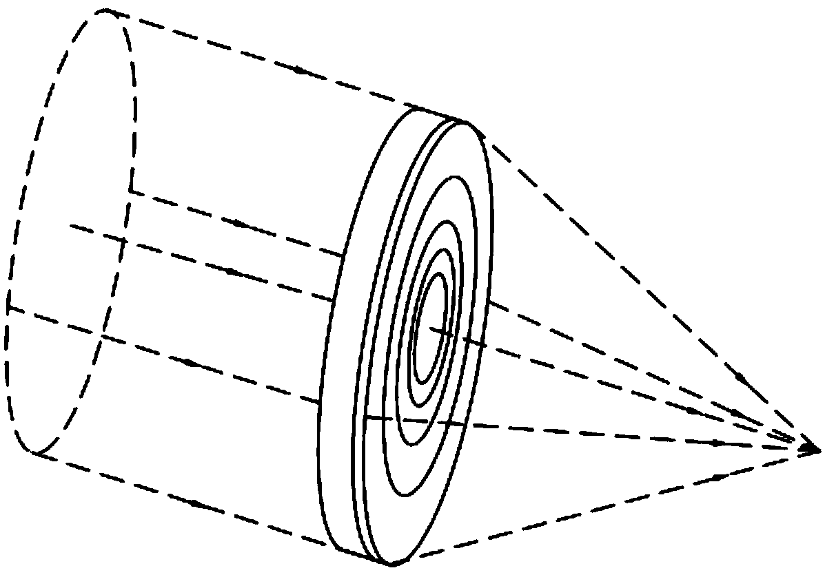
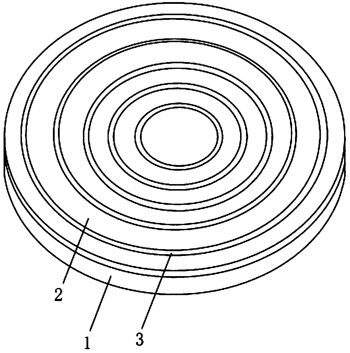
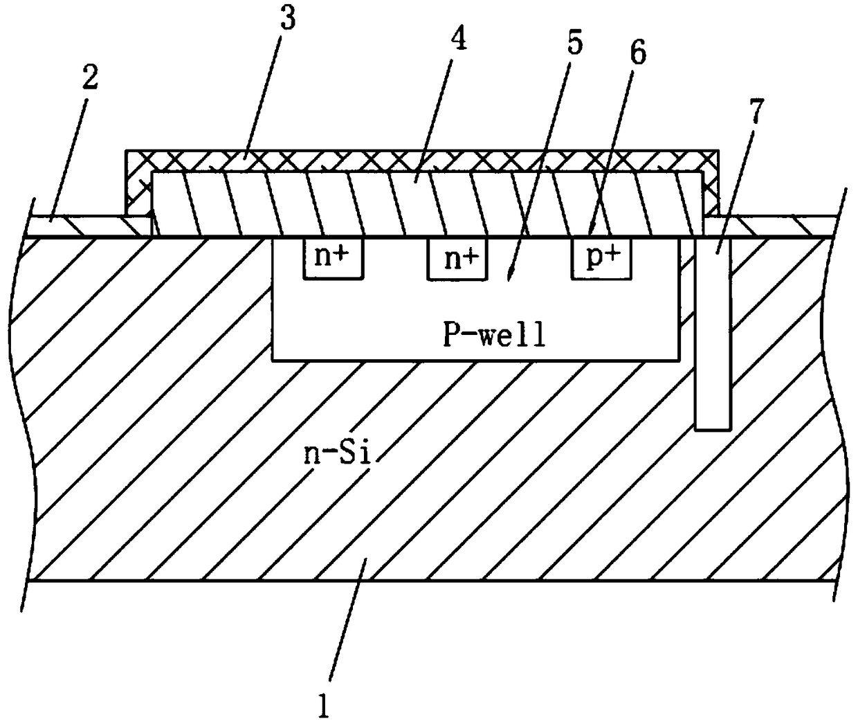
[0024] Embodiment: A reconfigurable terahertz wave super-diffraction focusing device based on voltage regulation, such as figure 2 and image 3 As shown, it includes a silicon layer 1 and a plurality of graphene layers 2 in contact with the surface of the silicon layer 1, and six graphene layers 2 are used in this embodiment. The graphene layer 2 is in the shape of a ring, six graphene layers 2 are arranged concentrically, and the distance between adjacent graphene layers 2 is equal. An insulating layer 4 adjoining the silicon layer 1 is arranged between adjacent graphene layers 2 , and the thickness of the insulating layer 4 is greater than that of the graphene layer 2 . The surface of the insulating layer 4 is covered with a conductive layer 3 , and both sides of the conductive layer 3 are in contact with the adjacent graphene layer 2 respectively. The conductive layer 3 is made of conductive metal.

[0025] Such as figure 1 and figure 2 As shown, using six ring-shape...


PUM


Abstract

The invention discloses a reconfigurable TeraHertz wave super-diffraction focusing device based on voltage regulation and control, relates to the technical field of TeraHertz wave focusing, and solvesthe problems that an existing TeraHertz wave technology is based on a near-field optics principle although super-resolution focusing is realized, and focal length is extremely small so as to be difficult in meeting far-field high-resolution optical focusing requirements of application fields including biomedical imaging, remote sensing, security check and the like. The device has the technical scheme key point that the device comprises a silicon layer and a plurality of graphene layers abutted against the surface of the silicon layer, wherein the graphene layers are annular and are concentrically arranged, and adjacent graphene layers have the same interval; an insulation layer abutted against the silicon layer is arranged between the adjacent graphene layers; an electric conduction layercoats the surface of the insulation layer; and two sides of the electric conduction layer are independently abutted against the adjacent graphene layers. TeraHertz wave diffraction limitation is broken through, and a far-field high-resolution optical focusing effect is achieved.

Description

technical field [0001] The invention relates to the technical field of terahertz wave focusing, more specifically, it relates to a reconfigurable terahertz wave super-diffraction focusing device based on voltage regulation. Background technique [0002] Terahertz waves refer to electromagnetic waves with a frequency of 0.1-10 THz. This band contains rich spectral information, such as the rotation / oscillation spectrum of macromolecules including proteins, and the lattice vibration energy spectrum of solid materials. Compared with microwaves and light waves, terahertz waves have the characteristics of low energy, strong penetrating power, high safety, and rich spectral information, and have important application prospects in nondestructive testing, security inspection, medical imaging, and communication. [0003] The development of terahertz technology has put forward higher requirements for the focusing spot and imaging resolution in the terahertz band. In recent years, some...

Claims


Application Information

Patent Timeline
IPC IPC(8): G02B27/42
CPCG02B27/4233
Inventor 温中泉陈刚张智海梁高峰
Owner CHONGQING UNIV
Why Eureka
Try Eureka