Transistor and manufacturing method thereof

A manufacturing method and transistor technology, applied in semiconductor/solid-state device manufacturing, semiconductor devices, electrical components, etc., can solve problems such as unstable device amplification factor, and achieve the effect of improving device yield and stabilizing the amplification factor

Inactive Publication Date: 2018-12-18
SHENZHEN NANSHUO MINGTAI TECH CO LTD
View PDF4 Cites 1 Cited by
  • Summary
  • Abstract
  • Description
  • Claims
  • Application Information

AI Technical Summary

Problems solved by technology

On the contact surface of the base region and the emitter region, a large number of processes will be experienced, especially the lithography and etching of the base region window and the lithography and etching of the emitter window, which will bring a large number of defects to the surface of the base region, and finally The amplification factor of the device is very unstable

Method used


Image

  • Transistor and manufacturing method thereof
  • Transistor and manufacturing method thereof
  • Transistor and manufacturing method thereof

Examples


Embodiment Construction

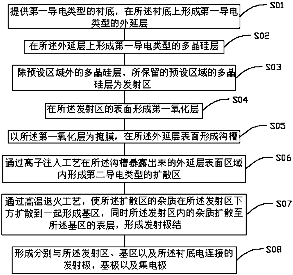
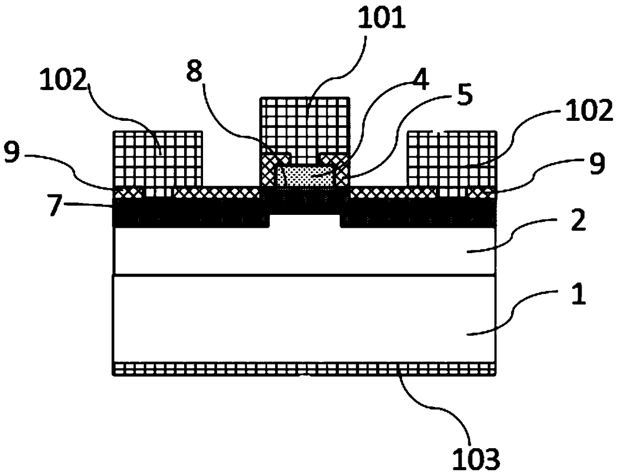
[0013] In order to make the objectives, technical solutions and beneficial technical effects of the present invention clearer, the technical solutions in the embodiments of the present invention will be clearly and completely described below in conjunction with the drawings in the embodiments of the present invention. Obviously, the described implementation Examples are only some embodiments of the present invention, not all embodiments. Based on the embodiments of the present invention, all other embodiments obtained by persons of ordinary skill in the art without making creative efforts belong to the protection scope of the present invention.

[0014] It should be noted that, in the case of no conflict, the embodiments of the present invention and the features in the embodiments can be combined with each other.

[0015] In describing the present invention, it should be understood that the terms "center", "longitudinal", "transverse", "upper", "lower", "front", "rear", "left"...


PUM


Abstract

The invention relates to a transistor and a manufacturing method thereof. The method comprises the following steps: providing a substrate of a first conductivity type; forming an epitaxial layer of the first conductivity type on the substrate; forming a polysilicon layer of a first conductivity type on the epitaxial layer; removing a polycrystalline silicon layer outside the preset region, whereinthe polycrystalline silicon layer retained in the preset region is an emitter region; forming a first oxide layer on the surface of the emission region; forming a trench on the surface of the epitaxial layer using the first oxide layer as a mask; and forming a diffusion region of a second conductivity type in a surface region of the epitaxial layer exposed by the trench by an ion implantation process. Through a high-temperature annealing process, the impurities in the diffusion region are diffused together under the emitter region to form a base region, and simultaneously, the impurities in the emitter region are diffused to the surface layer of the base region to form an emitter junction; and the transistor formed by the method has a good interface state between the base region and the emitter region, and the amplification coefficient is stable.

Description

technical field [0001] The invention relates to the technical field of semiconductors, in particular to a transistor and a manufacturing method thereof. Background technique [0002] In the prior art, the base region is formed by an annealing process after the implantation process, and the junction depth and junction morphology of the base area are greatly affected by the annealing process, while the polycrystalline emitter process is all implanted with a large dose in the polycrystalline body, and then high temperature and rapid Thermal annealing, so that impurities diffuse into the base region to form the emitter junction. On the contact surface of the base region and the emitter region, a large number of processes will be experienced, especially the lithography and etching of the base region window and the lithography and etching of the emitter window, which will bring a large number of defects to the surface of the base region, and finally The amplification factor of th...

Claims


Application Information

Patent Timeline
Patent Type & Authority Applications(China)
IPC IPC(8): H01L21/331H01L29/735
CPCH01L29/6625H01L29/735
Inventor 不公告发明人
Owner SHENZHEN NANSHUO MINGTAI TECH CO LTD
Why Eureka
Try Eureka