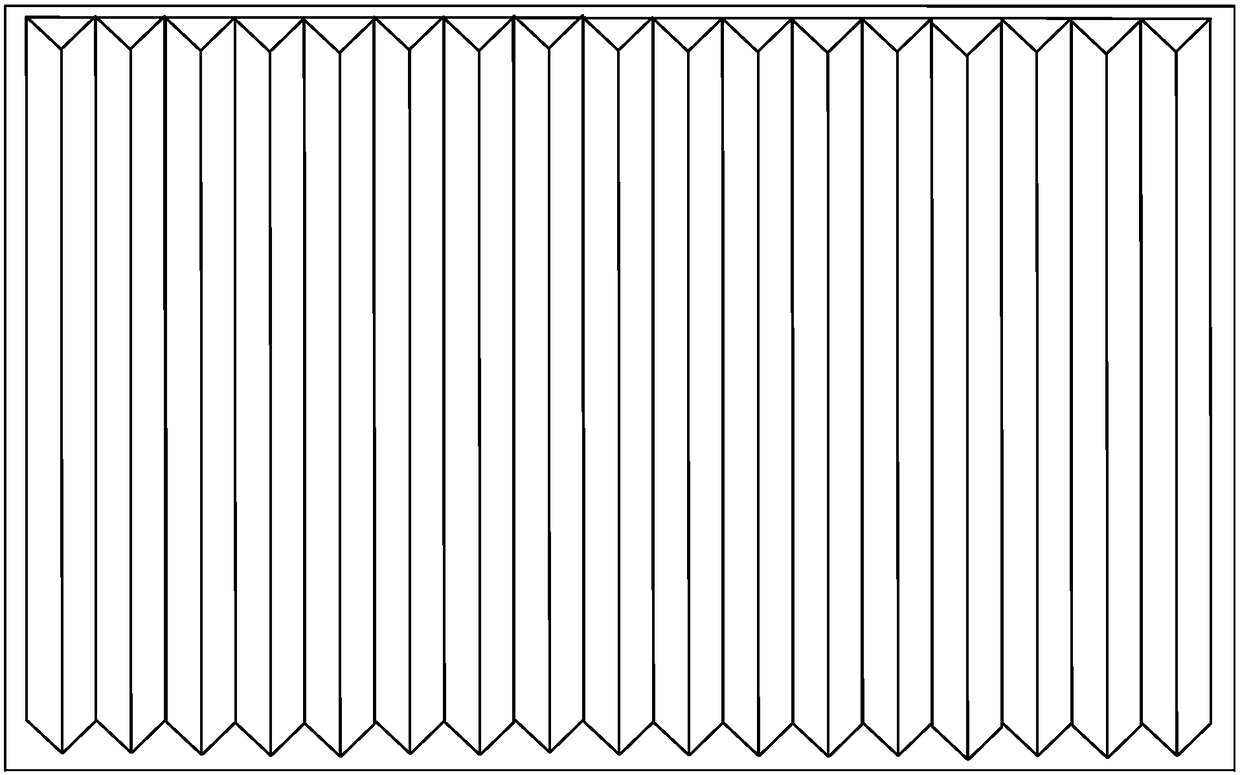
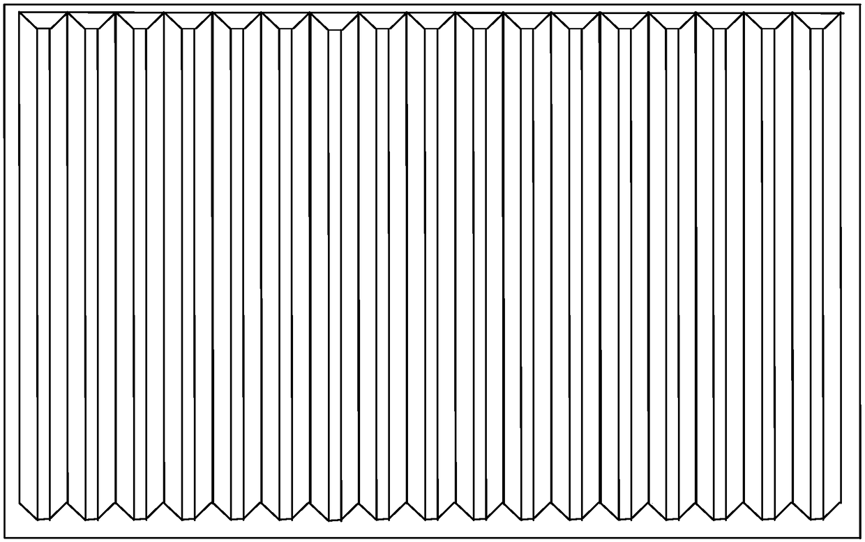
An adhesive film for photovoltaic modules having a pattern directionally reflecting light on the surface and having a cross-linked surface cured with ultraviolet light
A directional reflection, photovoltaic module technology, applied in photovoltaic power generation, electrical components, semiconductor devices, etc., can solve the problem of limited power of the module, and achieve the effect of improving the power of the module, increasing the utilization rate, and reducing the cost of the module
- Summary
- Abstract
- Description
- Claims
- Application Information
AI Technical Summary
Problems solved by technology
Method used
Image
Examples
Embodiment 1
[0034] Add 3% photoinitiator benzophenone, 10% barium sulfate, 20% titanium dioxide and other components to the EVA resin, and mix well. The mixture is melted and extruded in the extruder, and the temperature is controlled at 85°C. The extruded product is cast into a single-layer white film, and the white EVA film battery is embossed into a triangular prism pattern. The depth is 500 μm, the width is 866 μm, the top angle is 160°, the bottom angle is 10°, the angle between the triangular prism pattern and the extrusion direction of the film is 90°, and the film thickness is 0.50 mm. The formed white EVA film is used with a radiation intensity of 2000W / m 2 The ultraviolet lamp is irradiated for 100s to carry out ultraviolet curing and cross-linking. After irradiation, the thickness of the cross-linked surface layer is 0.01 mm, and the degree of cross-linking is 85%.
[0035] Place the white EVA adhesive film in the above example 1 on the back of the cell in the single glass mod...
Embodiment 2
[0037] Add 0.5% photoinitiator 2-methyl-2-(4-morpholinyl)-1-[4-(methylthio)phenyl]-1-acetone, 0.5% photoinitiator in EVA resin 4-methylbenzophenone, 0.1% titanium dioxide and other components, and mix well. The mixture is melted and extruded in the extruder, and the temperature is controlled at 80°C. The extruded product is cast into a white translucent film, and the white translucent EVA film battery is embossed into a square prism pattern. The film thickness was 0.55 mm. The formed white translucent EVA film is used with a radiation intensity of 2000W / m 2 Ultraviolet light is irradiated for 60s to carry out ultraviolet curing and crosslinking. After irradiation, the thickness of the cured and crosslinked surface layer is 0.10 mm, and the degree of crosslinking is between 65% and 75%.
[0038] Place the white translucent EVA adhesive film in the above example 2 on the back of the battery sheet in the double-glass module, and place the triangular prism-shaped embossed surfac...
Embodiment 3
[0040]A double-layer co-extrusion EVA film solution is adopted, one layer of EVA is silver, and 5% of glass beads with metal coating, 0.6% of photoinitiator diaryliodonium salt and other components are added to the EVA resin; One layer of EVA is transparent, using conventional transparent formula. The above components are fully mixed respectively and then added to a double-layer co-extrusion extruder (two extruders) to form a film. When extruding, one side of the silver EVA film battery is embossed into a triangular pyramid pattern. The depth of the pyramid-shaped pattern is 10 μm, the apex angle of the side triangle is 170°, and the thickness of the adhesive film is 0.70 mm. The silver EVA film that will be formed will use a radiation intensity of 2000W / m 2 Ultraviolet light is irradiated for 30s to carry out ultraviolet curing and crosslinking. After irradiation, the thickness of the crosslinked surface layer is 0.05mm, and the degree of crosslinking is between 30% and 40%....
PUM
| Property | Measurement | Unit |
|---|---|---|
| Surface thickness | aaaaa | aaaaa |
| Angle | aaaaa | aaaaa |
| Depth | aaaaa | aaaaa |
Abstract
Description
Claims
Application Information


