Semiconductor device and forming method thereof

A semiconductor and device technology, applied in the field of semiconductor devices and their formation, can solve problems such as poor performance of semiconductor devices, and achieve the effect of improving performance and avoiding leakage

Active Publication Date: 2019-01-04
SEMICONDUCTOR MANUFACTURING INTERNATIONAL (BEIJING) CORP +1
View PDF6 Cites 0 Cited by
  • Summary
  • Abstract
  • Description
  • Claims
  • Application Information

AI Technical Summary

Problems solved by technology

[0004] However, the performance of semiconductor devices composed of existing fin field effect transistors is poor

Method used


Image

  • Semiconductor device and forming method thereof
  • Semiconductor device and forming method thereof
  • Semiconductor device and forming method thereof

Examples


Embodiment Construction

[0032] As mentioned in the background, semiconductor devices formed in the prior art have poor performance.

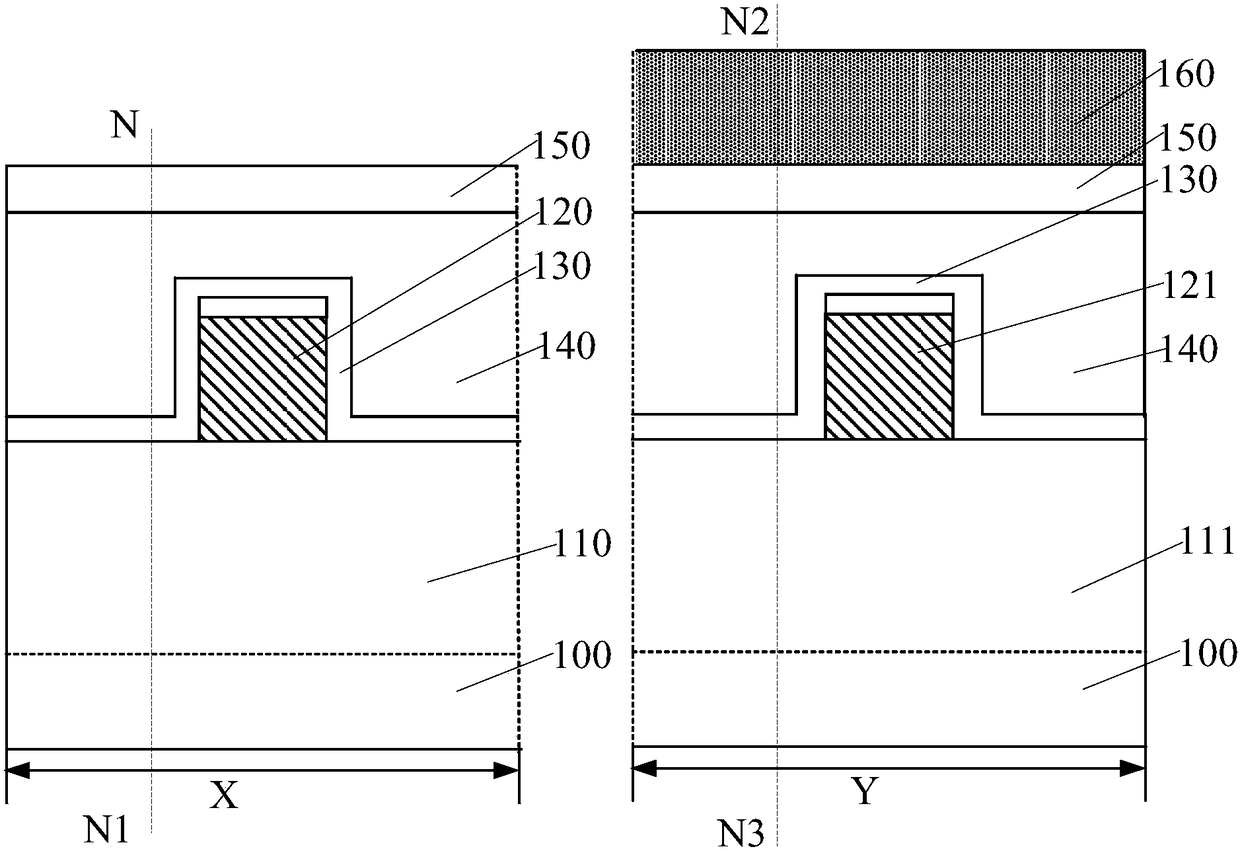
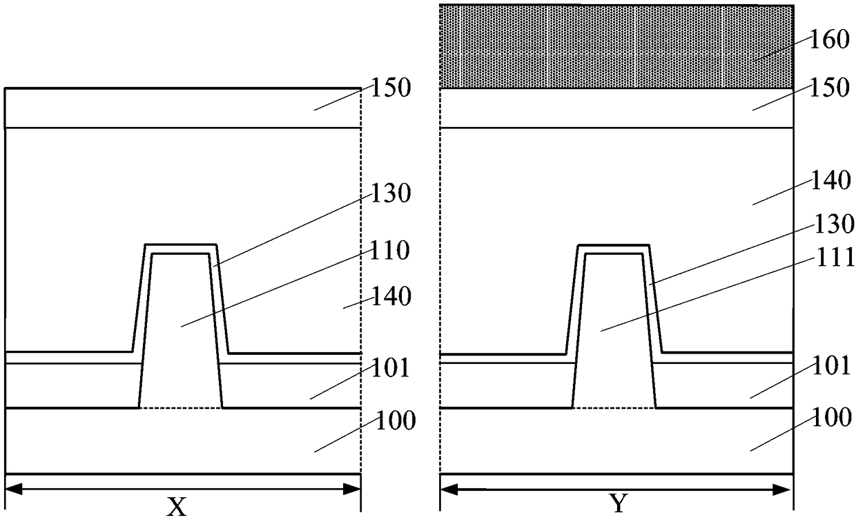
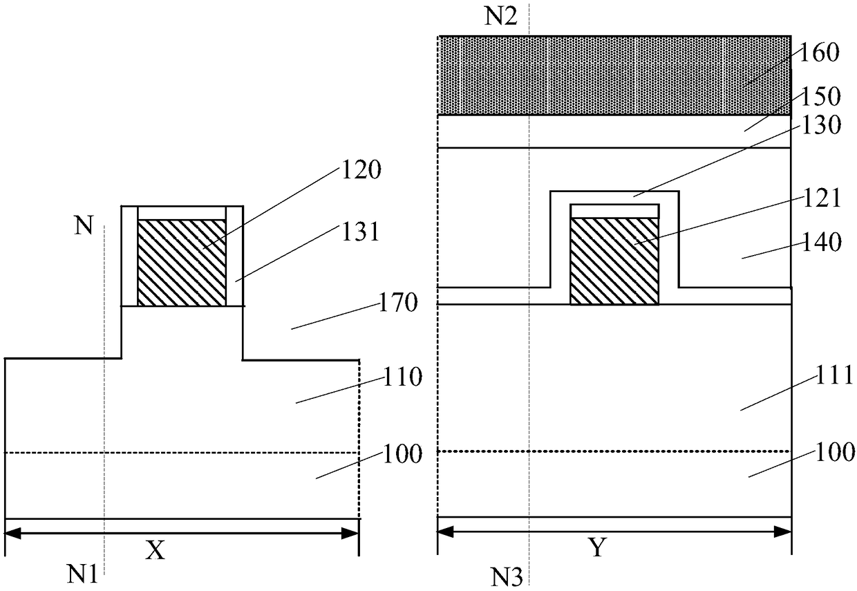
[0033] Figure 1 to Figure 4 It is a structural schematic diagram of the formation process of a semiconductor device.

[0034] combined reference figure 1 and figure 2 , figure 2 The diagram of the first zone in the figure 1 obtained by cutting the line N-N1, figure 2 The illustration of the second zone in the figure 1 Obtained by cutting line N2-N3 in the center, a substrate 100 is provided, the substrate 100 includes a first region X and a second region Y, the first region X of the substrate 100 has a first fin 110, and the second region Y of the substrate 100 There is a second fin 111 on the substrate 100, and an isolation structure 101 covering a part of the sidewall of the first fin 110 and a part of the sidewall of the second fin 111 is formed on the substrate 100; A gate structure 120, the first gate structure 120 straddles the first fin 110, covers ...


PUM


Abstract

A semiconductor device and a forming method thereof, wherein the method comprises forming a first sidewall film on a sidewall of a first gate structure and a second region; forming a first flat layeron a first sidewall film surface of the first region and a second region, and on an isolation structure, the entire top surface of the first planar layer of the first region being lower than the top surface of the first fin; forming a first filling layer on the surface of the first planar layer, the exposed surface of the first sidewall film, the first fin and the first gate structure, the entiresurface of the first filling layer in the first region being higher than the top surface of the first gate structure, and the hardness of the first filling layer being greater than that of the first planar layer; forming a first photoresist layer on the surface of the first filling layer of the second region, the first photoresist layer exposing the first filling layer of the first region; etchingthe first filling layer, a first fin portion, and a first planar layer using the first photoresist layer as a mask to form a first depression in the first fin portion. The method improves the performance of the semiconductor device.

Description

technical field [0001] The invention relates to the field of semiconductor manufacturing, in particular to a semiconductor device and a forming method thereof. Background technique [0002] MOS transistors are one of the most important components in modern integrated circuits. The basic structure of a MOS transistor includes: a semiconductor substrate; a gate structure located on the surface of the semiconductor substrate, a source region located in the semiconductor substrate on one side of the gate structure, and a drain region located in the semiconductor substrate on the other side of the gate structure. The working principle of the MOS transistor is: by applying a voltage to the gate structure, the current through the channel at the bottom of the gate structure is adjusted to generate a switching signal. [0003] With the development of semiconductor technology, the ability of the traditional planar MOS transistor to control the channel current becomes weaker, resultin...

Claims


Application Information

Patent Timeline
IPC IPC(8): H01L21/336H01L21/28H01L29/10H01L29/423H01L29/78
CPCH01L29/1033H01L29/42356H01L29/66795H01L29/785
Inventor 李勇
Owner SEMICONDUCTOR MANUFACTURING INTERNATIONAL (BEIJING) CORP
Why Eureka
Try Eureka